Charged particle beam device

a charge-particle and beam technology, applied in the field of charge-particle beam devices, can solve the problems of not disclosing at all the internal configuration, not disclosing at all the chromatic aberration correction, and complicated operation of a multi-pole, etc., to achieve better operability, simple device configuration, and good operability

Active Publication Date: 2009-03-17
HITACHI HIGH-TECH CORP
View PDF23 Cites 13 Cited by
  • Summary
  • Abstract
  • Description
  • Claims
  • Application Information

AI Technical Summary

Benefits of technology

[0007]In view of the above situation, the object of the present invention is to provide a charged particle beam device provided with an aberration corrector which has a simpler device configuration and better operability than conventional one and is capable of correcting a chromatic aberration and / or a spherical aberration.
[0008]In a charged particle beam device having an aberration correction means, a multi-hole stop is used at the time of adjusting the aberration correction means and scanning charged particle beam images (for example, SEM images or SIM images) are formed with plurally divided beams. A specimen is scanned with plural beams and hence overlapping images are obtained. Then it is possible to correct the chromatic aberration and the spherical aberration with good operability by judging the correction state of the aberrations from the directions and symmetry of the overlapping and feeding back the judgment result to the adjustment of the aberration corrector so as to eliminate the overlapping. Further, it is possible to secure a deep focal depth by using an orbicular zone aperture the center of which is shielded in the state of the aberration correction.
[0009]The optical axis of a charged particle beam supplied from an identical charged particle source is divided into plurality, and an aberration corrector is adjusted so that the plurally divided optical axes are superimposed. Since the degree of the adjustment of the aberration corrector is visually observed, the operability of the adjustment of the aberration corrector improves outstandingly. Further, since the process of the adjustment under the visual observation can easily be replaced with image processing, the measure is suitable for the automation of the adjustment of the aberration corrector.

Problems solved by technology

When an aberration corrector is used, how to actually adjust a multipole is important and the operation of a multipole is complicated and requires sufficient experiences.
For example, the aforementioned Published Japanese Translation of PCT No. 521801 / 2003 does not disclose at all the chromatic aberration correction which is necessary as the preliminary step of spherical aberration correction.
Further, the aforementioned Published Japanese Translation of PCT No. 505899 / 2005 only describes that “astigmatism can be corrected with an astigmatic corrector” and does not disclose at all the internal configuration of the astigmatic corrector and the concrete adjustment method thereof.

Method used


Image

  • Charged particle beam device
  • Charged particle beam device
  • Charged particle beam device

Examples


first embodiment

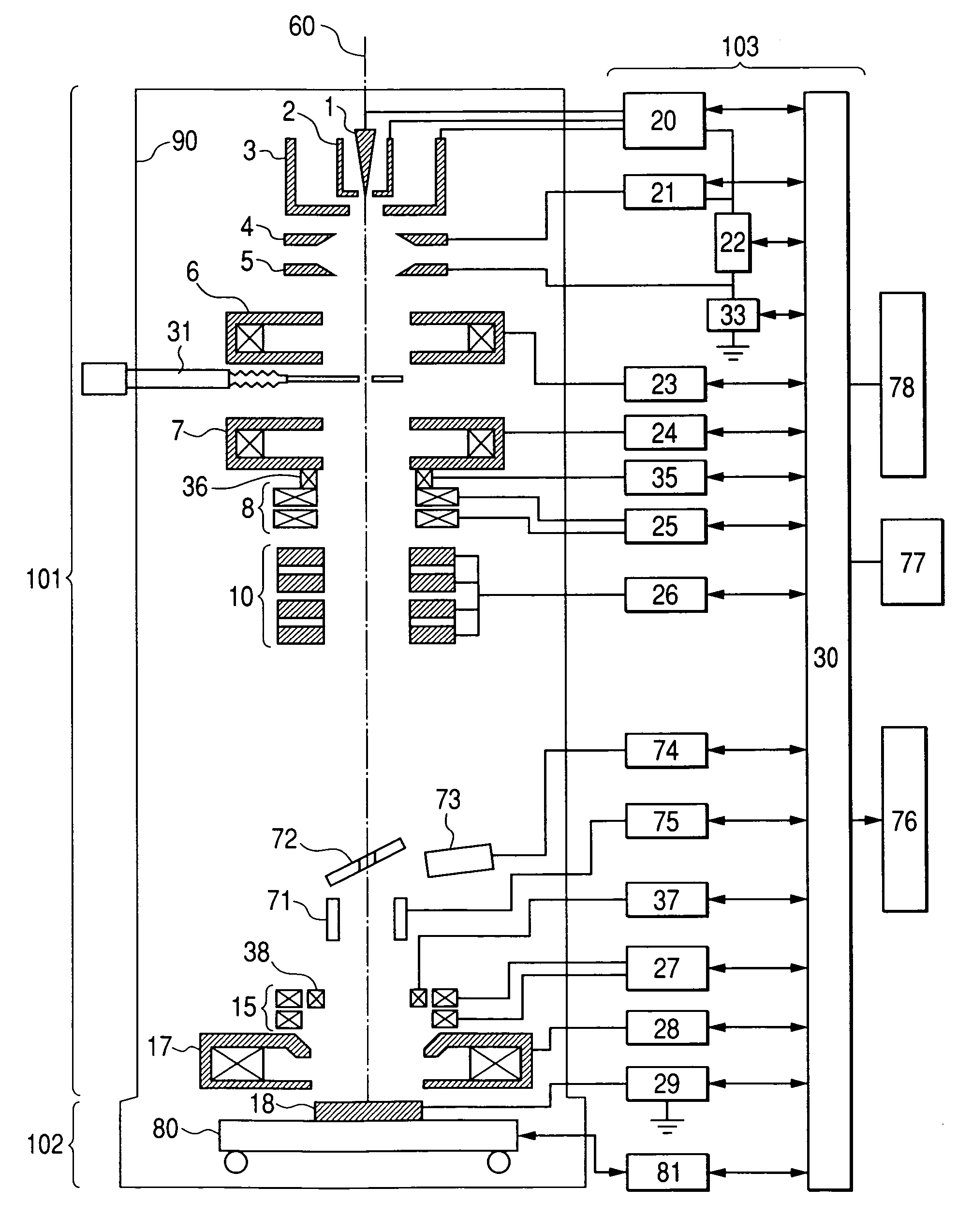
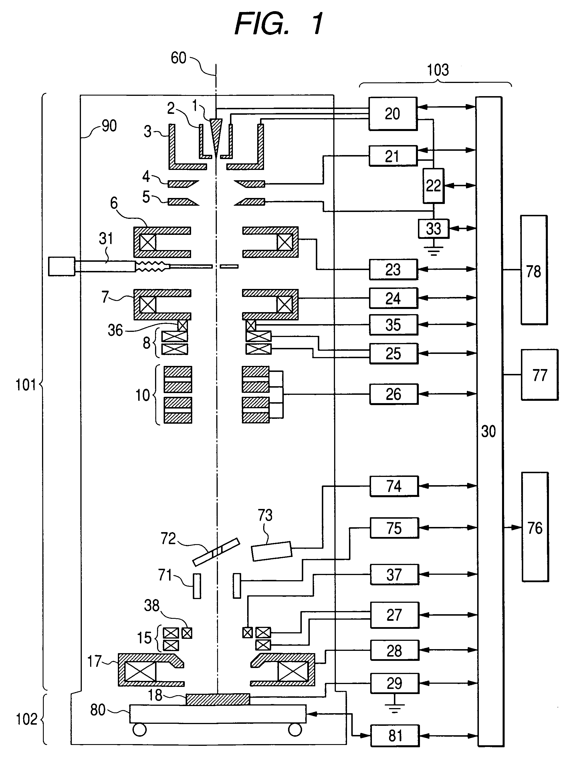
[0022]FIG. 1 shows a general configuration of a scanning electron microscope as an embodiment according to the present invention. The scanning electron microscope of the present embodiment is roughly composed of: a SEM column 101 to irradiate or scan a specimen with an electron beam; a specimen chamber 102 to contain a specimen stage; a control unit 103 to control components of the SEM column 101 and the specimen chamber 102; and others. Further, to the control unit 103, connected are: a data storage 76 to store prescribed information; a monitor 77 to display obtained images; and an operator console 78 to function as a man-machine interface between the device and device users. The operator console comprises information input means such as a keyboard, a mouse and the like, for example.

[0023]Firstly, the components in the SEM column 101 are explained. A Schottky electron source 1 is an electron source which is made by diffusing oxygen, zirconium and others in a monocrystal of tungsten...

second embodiment

[0047]The present embodiment is explained on the basis of a case where the present invention is applied to a critical-dimension-measurement SEM (scanning electron microscope). As a specimen for dimension measurement, a semiconductor wafer or a semiconductor chip on which a circuit pattern is formed, or a specimen produced by cutting out a part of the wafer may be adopted.

[0048]FIG. 8 shows the configuration of the hardware of a critical-dimension-measurement SEM in the present embodiment. The general configuration of the critical-dimension-measurement SEM is the same as that of the charged particle beam application device explained in the first embodiment in the fact that the critical-dimension-measurement SEM is composed of: a SEM column 101; a specimen chamber 102 to contain a specimen stage; a control unit 103; and others. However, the critical-dimension-measurement SEM has a specimen preparation chamber (load chamber) 40 to introduce a specimen to be subjected to dimension measu...


PUM


Abstract

A scanning charged particle microscope which facilitates adjustment, has a deep focal depth, and is provided with an aberration correction means. The state of aberration correction is judged from a SEM image by using a stop having plural openings and the judgment result is fed back to the adjustment of the aberration correction means. A stop of a nearly orbicular zone shape is used in combination with the aberration correction means.

Description

CLAIM OF PRIORITY[0001]The present application claims priority from Japanese application JP 2005-140588 filed on May 13, 2005, the content of which is hereby incorporated by reference into this application.FIELD OF THE INVENTION[0002]The present invention relates to a charged particle beam device, in particular to a scanning electron microscope, an electron beam semiconductor inspector, an electron beam semiconductor dimension measurement device, a focused ion beam device and the like, each of which has an aberration corrector.BACKGROUND OF THE INVENTION[0003]A scanning electron microscope (SEM) has a higher resolution than an optical microscope in the observation of the surface of an object, and hence it is widely used not only as a device for research but also as an industrial device for the dimension measurement of semiconductor wafer patterns which have increasingly been miniaturized in recent years, the observation of foreign matters on a surface and the like. In the case of th...

Claims


Application Information

Patent Timeline
Patent Type & Authority Patents(United States)
IPC IPC(8): G21K7/00
CPCH01J37/153H01J2237/0453
Inventor KAWASAKI, TAKESHINAKANO, TOMONORIHATANO, MICHIOENYAMA, MOMOYO
Owner HITACHI HIGH-TECH CORP
Why Eureka
Try Eureka