Method and apparatus for automatically detecting and correcting misalignment of a semiconductor chip
- Summary
- Abstract
- Description
- Claims
- Application Information
AI Technical Summary
Benefits of technology
Problems solved by technology
Method used
Image


Examples
Embodiment Construction
[0022]The following description is presented to enable any person skilled in the art to make and use the invention, and is provided in the context of a particular application and its requirements. Various modifications to the disclosed embodiments will be readily apparent to those skilled in the art, and the general principles defined herein may be applied to other embodiments and applications without departing from the spirit and scope of the present invention. Thus, the present invention is not limited to the embodiments shown, but is to be accorded the widest scope consistent with the principles and features disclosed herein.
Automatic Misalignment Detection and Correction
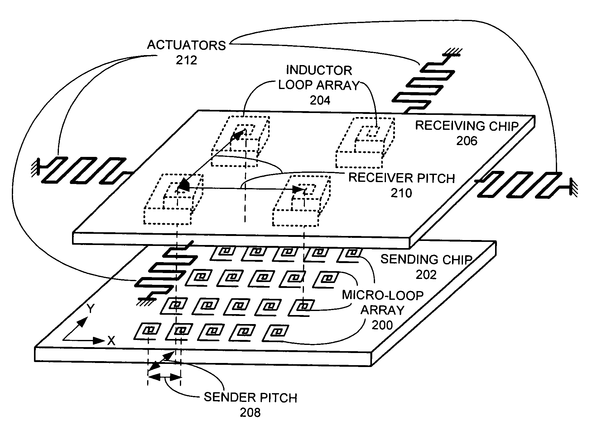
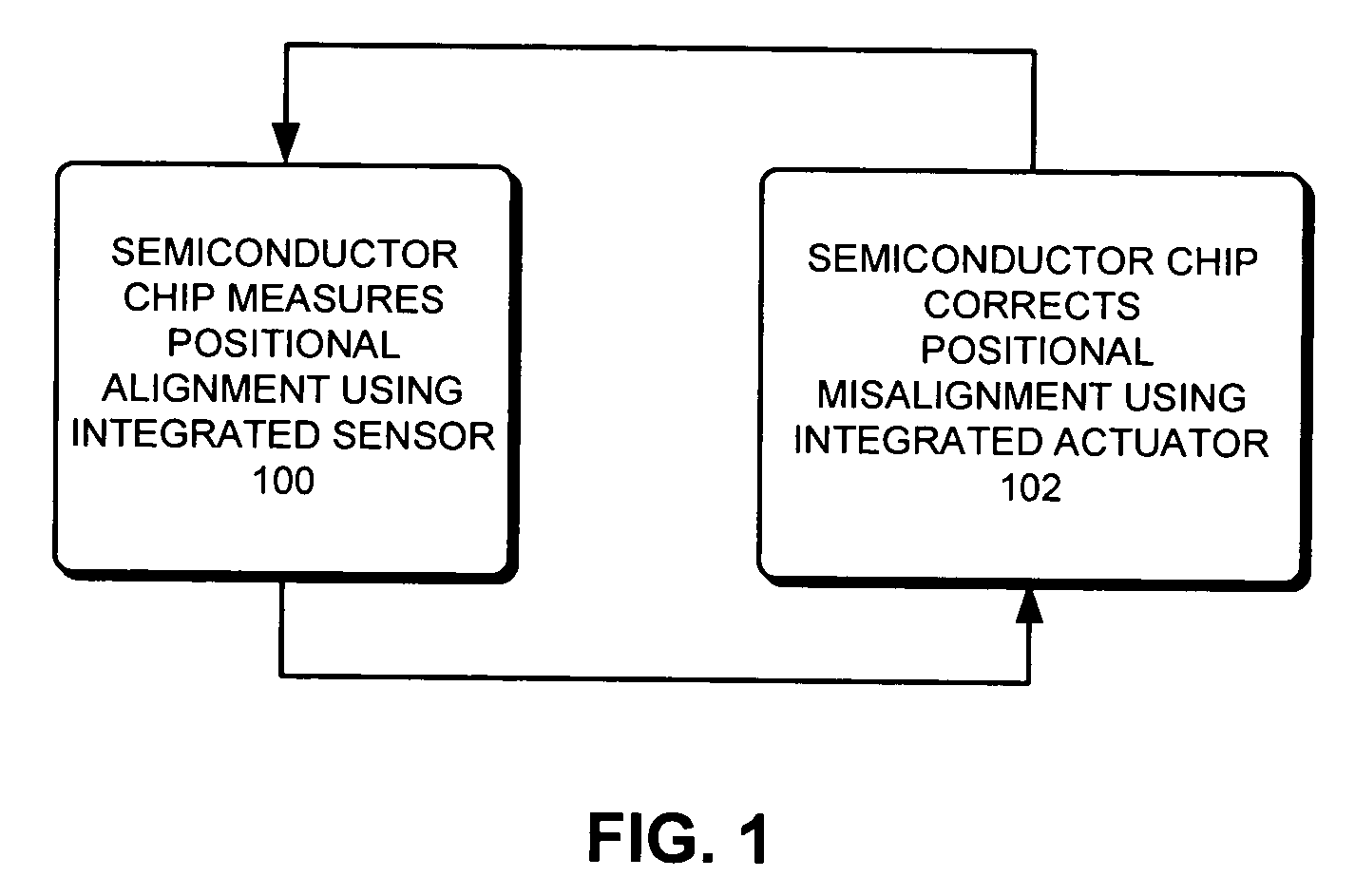
[0023]One embodiment of the present invention allows automatic detection and correction of a misalignment of a chip from a desired location on a chip carrier, such as a printed circuit board (PCB), thereby improving system performance and reliability. The alignment of the chip can be with respect to a neighboring...
PUM
| Property | Measurement | Unit |
|---|---|---|
| Electrical conductor | aaaaa | aaaaa |
| Contraction enthalpy | aaaaa | aaaaa |
| Thermal expansion coefficient | aaaaa | aaaaa |
Abstract
Description
Claims
Application Information