Method of Manufacturing Silicon Substrates for Magnetic Recording Medium, Silicon Substrate for Magnetic Recording Medium, Magnetic Recording Medium, and Magnetic Recording Apparatus

a technology of silicon substrates and magnetic recording mediums, which is applied in the manufacture of base layers, manufacturing tools, edge grinding machines, etc., can solve the problems of distortion layer being produced in the surface of the substrate, the distortion layer may be warped, and the substrate may be subjected to nip plating, etc., to achieve the effect of high speed, easy mass production of hard disk drives, and strict control of the dimensions of the center circular holes of silicon substrates

Inactive Publication Date: 2007-11-22
SHOWA DENKO KK
View PDF6 Cites 3 Cited by
  • Summary
  • Abstract
  • Description
  • Claims
  • Application Information

AI Technical Summary

Benefits of technology

[0021] In view of the above circumstances, an object of the present invention is to improve the accuracy and reduce dimensional variation of the inner diameters of the center circular holes of the silicon substrates, to efficiently manufacture silicon substrates suitable for hard disk drives which have consistent quality and can be rotated at high speed, and to provide a magnetic recording apparatus in which a magnetic recording medium using such silicon substrates is mounted.
[0033] According to the present invention, the accuracy in dimensions in center circular holes of silicon substrates is strictly regulated. Therefore, it is possible to easily mass-produce hard disk drives which have consistent quality and can be rotated at high speed.

Problems solved by technology

However, a substrate which has been subjected to NiP plating tends to be warped, and may be magnetized when being processed at a high temperature.
In addition, when the glass substrate is processed so as to be strengthened, a distortion layer may be produced in a surface of the substrate and the substrate may receive compressive stress, and the glass substrate also tends to be warped when being processed at a high temperature.
Regarding an ultra-small-sized magnetic recording medium having a diameter of 1 inch (i.e., 25.4 mm) or 0.85 inches (i.e., 21.6 mm) which requires higher recording density, warp of the substrate is a fatal problem.
The material for the silicon substrate is fragile; thus, cracks or chips tend to be produced in the above manufacturing processes.
When cracks or chips are produced, the yield rate for manufacturing the magnetic recording medium is reduced, and generated particles may cause errors in a write / read process, or a crash of the magnetic head in the write / read process.
Therefore, the accuracy for processing the center circular hole is important, and if this accuracy is inadequate, a problem may occur in assembling of a hard disk drive which can be rotated at high speed.
The silicon substrate is fragile; thus, a hard disk drive having high accuracy cannot be obtained by only limiting the surface roughness of the finished inner peripheral end face as shown in Reference 3.
With inadequate accuracy in dimensions of the inner diameters, it is impossible to mass-produce hard disk drives having consistent quality and high performance.
However, no trial or attempt for regulating the accuracy relating to the dimensional variation of the inner diameters of the center circular holes has been implemented.

Method used


Image

  • Method of Manufacturing Silicon Substrates for Magnetic Recording Medium, Silicon Substrate for Magnetic Recording Medium, Magnetic Recording Medium, and Magnetic Recording Apparatus
  • Method of Manufacturing Silicon Substrates for Magnetic Recording Medium, Silicon Substrate for Magnetic Recording Medium, Magnetic Recording Medium, and Magnetic Recording Apparatus
  • Method of Manufacturing Silicon Substrates for Magnetic Recording Medium, Silicon Substrate for Magnetic Recording Medium, Magnetic Recording Medium, and Magnetic Recording Apparatus

Examples


Embodiment Construction

[0046] Hereinbelow, the present invention will be explained in detail.

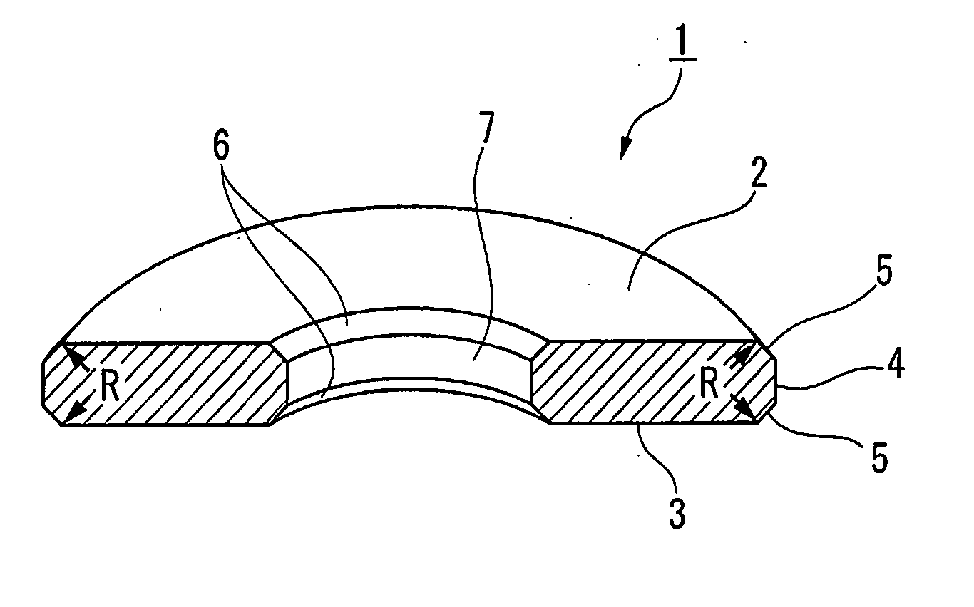
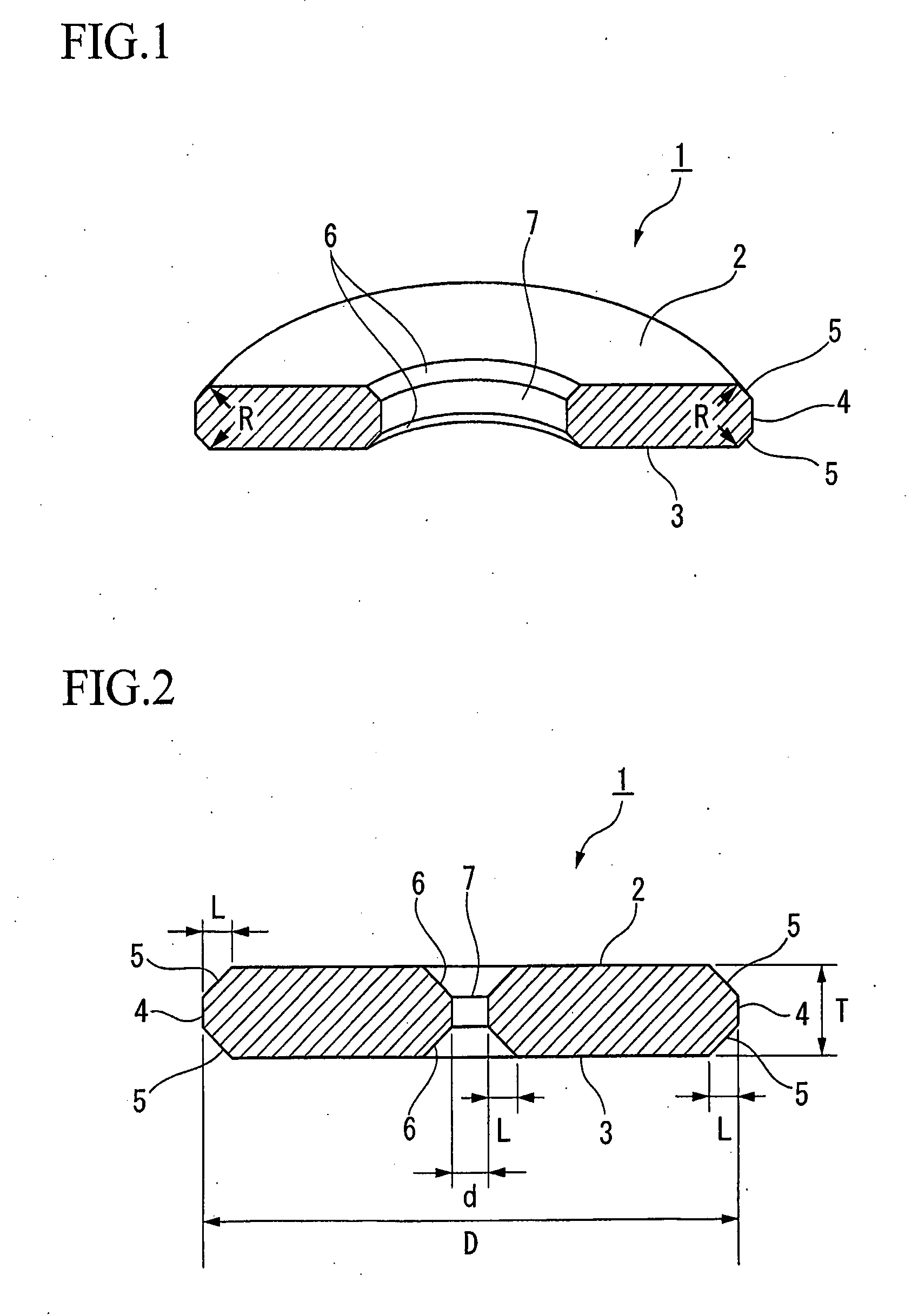
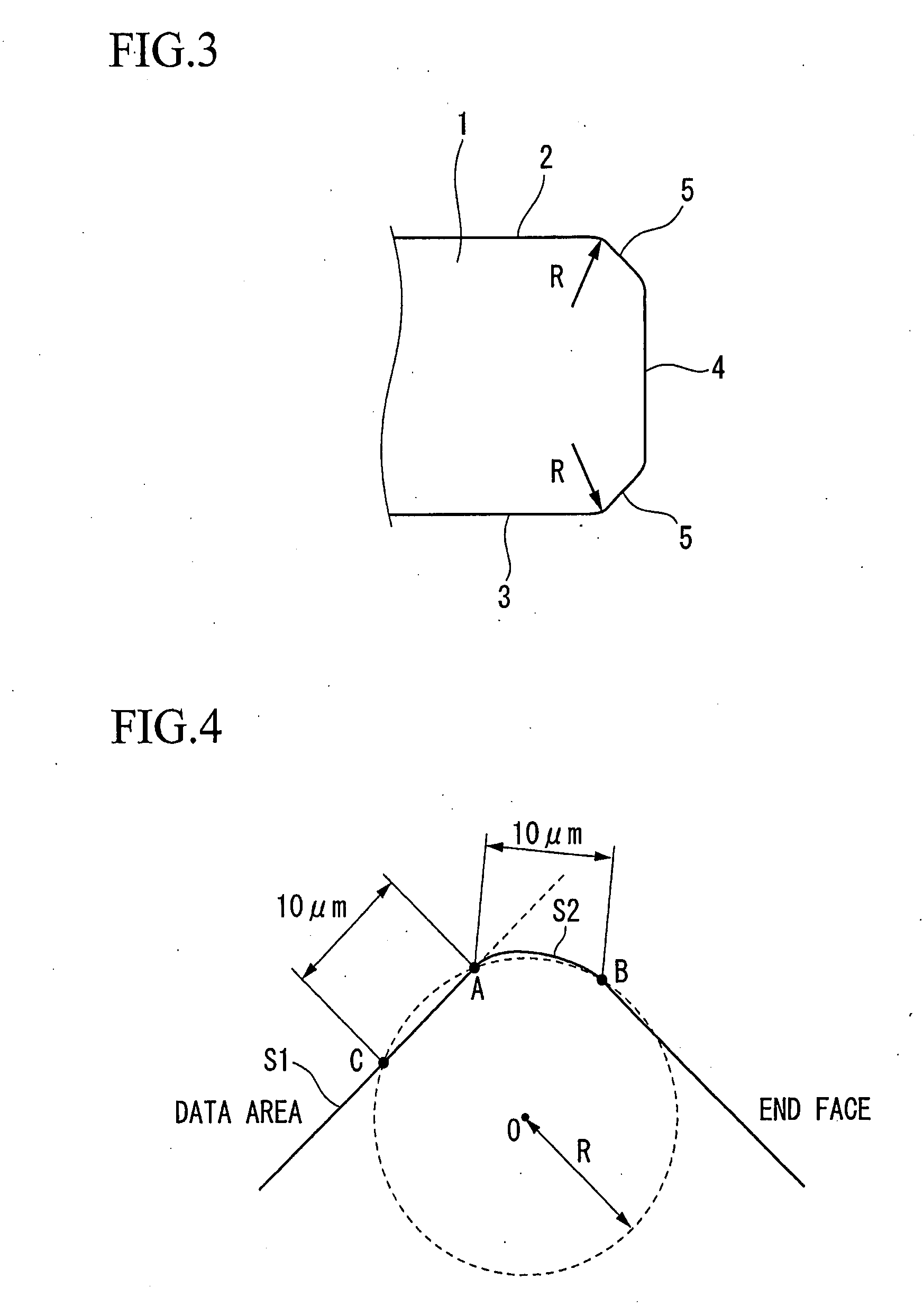
[0047]FIG. 1 is a perspective view of a silicon substrate for a magnetic recording medium according to the present invention, which is cut and viewed from the cut face. FIG. 2 is a diagram for explaining the dimension of each portion of the silicon substrate in FIG. 1 according to the present invention.

[0048] As shown in FIG. 1, the silicon substrate 1 for a magnetic recording medium according to the present invention forms a doughnut-shaped circular disk. The main surfaces 2 and 3 for implementing magnetic recording are formed on the front and back faces of the circular disk. The outer peripheral end face 4 is positioned at the outermost periphery of the circular disk, and the inner peripheral end face 7 is positioned at the inside of the center circular hole of the disk. Between the outer peripheral end face 4 and the main surfaces 2 and 3, outer peripheral chamfered portions 5 are formed, and inner peripheral...


PUM

PropertyMeasurementUnit
Diameteraaaaaaaaaa
Diameteraaaaaaaaaa
Lengthaaaaaaaaaa

Abstract

A manufacturing method for silicon substrates for a magnetic recording medium has the steps of forming a stack body of a number of silicon substrates which are stacked via spacers therebetween, wherein each silicon substrate has a circular hole at a center of the substrate; immersing the stack body of the silicon substrates in a polishing liquid in which grains are suspended; and polishing inner peripheral end faces of the circular holes of the silicon substrates, wherein in polishing, a polishing brush contacts the end faces while performing a relative rotation between the end faces and the polishing brush, and the stack body of the silicon substrates is inverted during polishing. The step of polishing the inner peripheral end faces may be performed before inner and outer peripheries of the silicon substrate are subjected to chamfering. Preferably, the polishing brush is made of polyamide resin.

Description

[0001] Priority is claimed on Japanese Patent Application No. 2004-237340, filed Aug. 17, 2004, and U.S. Provisional Patent Application No. 60 / 603,566, filed Aug. 24, 2004, the contents of which are incorporated herein by reference.TECHNICAL FIELD [0002] The present invention relates to a silicon substrate for a small-sized magnetic recording medium, which is used as a recording medium for a data processing apparatus. BACKGROUND ART [0003] Accompanying recent progress in data processing apparatuses, data recording capacity of a magnetic recording medium has increased more and more. In particular, in magnetic disks, which are important media as external memory for computers, both storage capacity and data recording density increase every year, and development for recording data with higher density is required. For example, in accordance with development of notebook computers or palmtop computers, small-sized and impact-resistant magnetic recording media are required, and therefore sm...

Claims


Application Information

Patent Timeline
IPC IPC(8): B24C1/08
CPCB24B9/065G11B5/8404B24B29/04B24B29/005
Inventor AIDA, KATSUAKI
Owner SHOWA DENKO KK
Why Eureka
Try Eureka