Flash memory with deep quantum well and high-K dielectric

a quantum well and flash memory technology, applied in the direction of semiconductor devices, basic electric elements, electrical appliances, etc., can solve the problems of significant leakage problems, stored charges can potentially leak through defects, and it is still difficult to scale the write/erase voltage below 5 v and maintain the required ten year data retention

Active Publication Date: 2007-11-29
TAIWAN SEMICON MFG CO LTD
View PDF19 Cites 47 Cited by
  • Summary
  • Abstract
  • Description
  • Claims
  • Application Information

AI Technical Summary

Problems solved by technology

However, conventional one-transistor flash memory has a conductive storage layer, and thus thin tunneling oxide layers will cause a significant leakage problem.
Particularly, if there is a defect in the tunneling oxide layer, all stored charges can potentially leak through the defect since charges can flow freely in the floating gate.
Although the SONOS memory devices provide a potential solution for down-scaling the tunneling oxide layer below conventional memory devices wit

Method used


Image

  • Flash memory with deep quantum well and high-K dielectric
  • Flash memory with deep quantum well and high-K dielectric
  • Flash memory with deep quantum well and high-K dielectric

Examples


Embodiment Construction

[0020]The making and using of the presently preferred embodiments are discussed in detail below. It should be appreciated, however, that the present invention provides many applicable inventive concepts that can be embodied in a wide variety of specific contexts. The specific embodiments discussed are merely illustrative of specific ways to make and use the invention, and do not limit the scope of the invention.

[0021]A manufacturing process of a preferred embodiment of the present invention is discussed. Variations of the preferred embodiments are provided, wherein like reference numbers are used to designate like elements throughout the various views and illustrative embodiments of the present invention. The operations of the preferred embodiments of the present invention are then discussed.

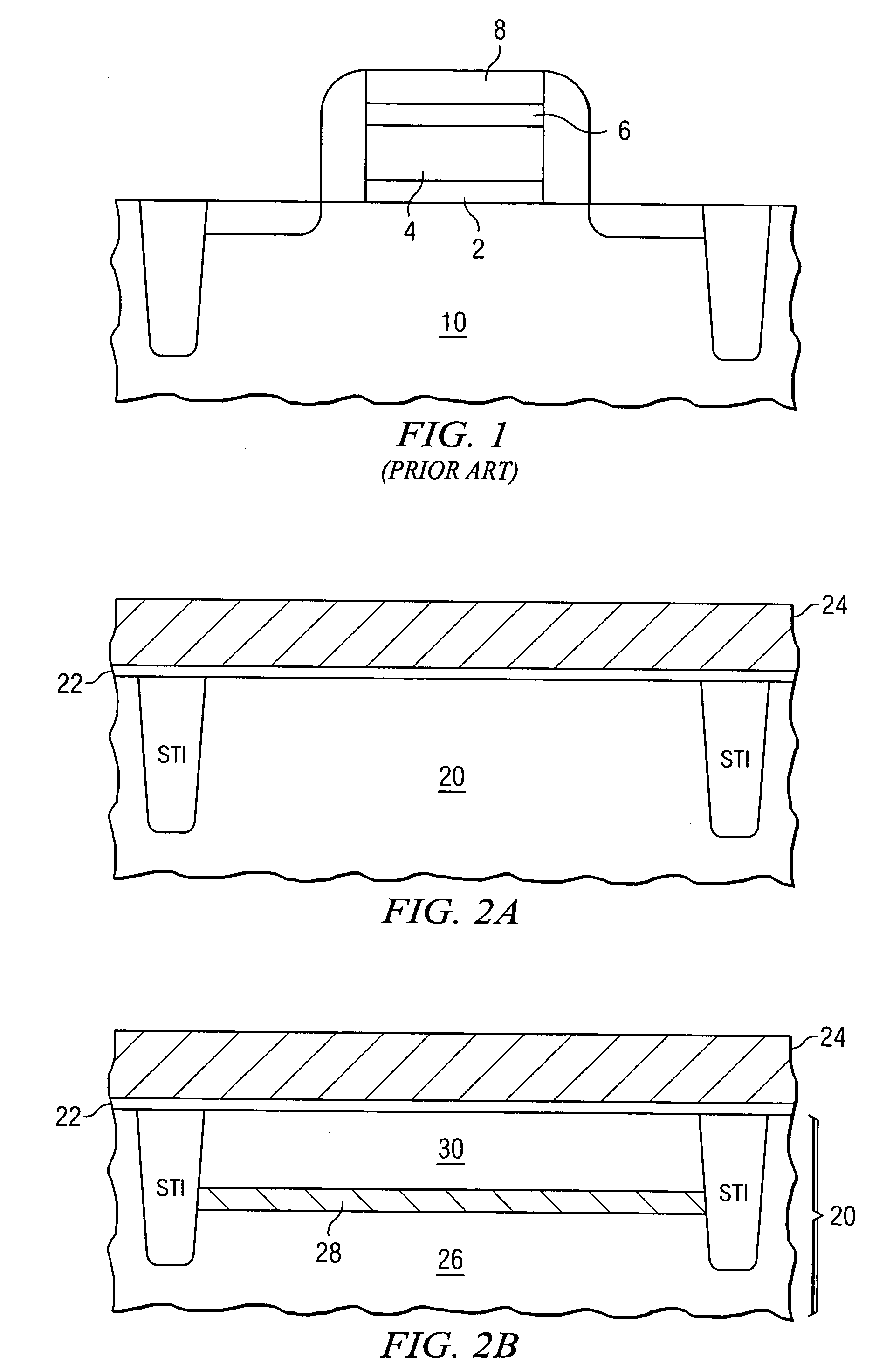
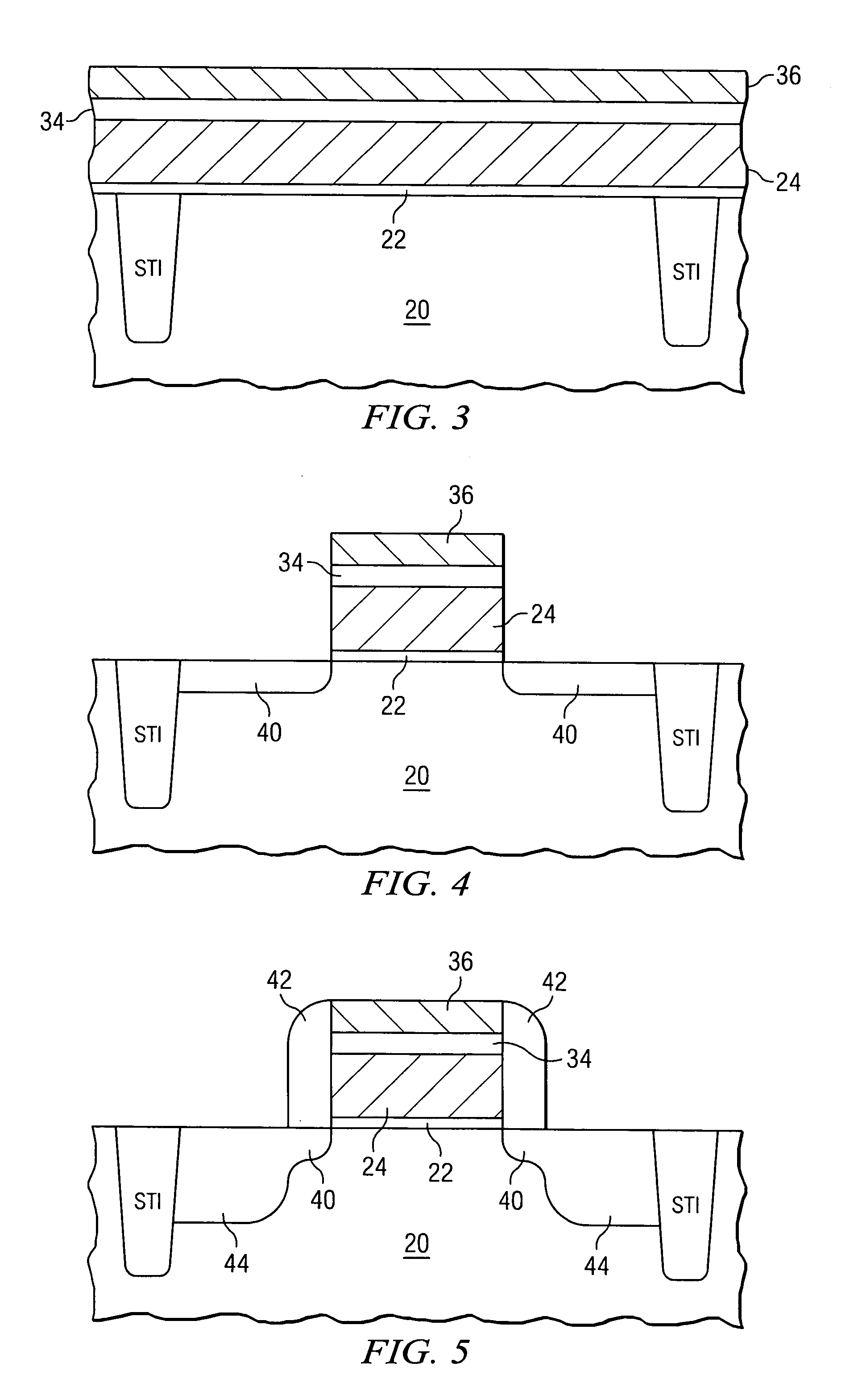
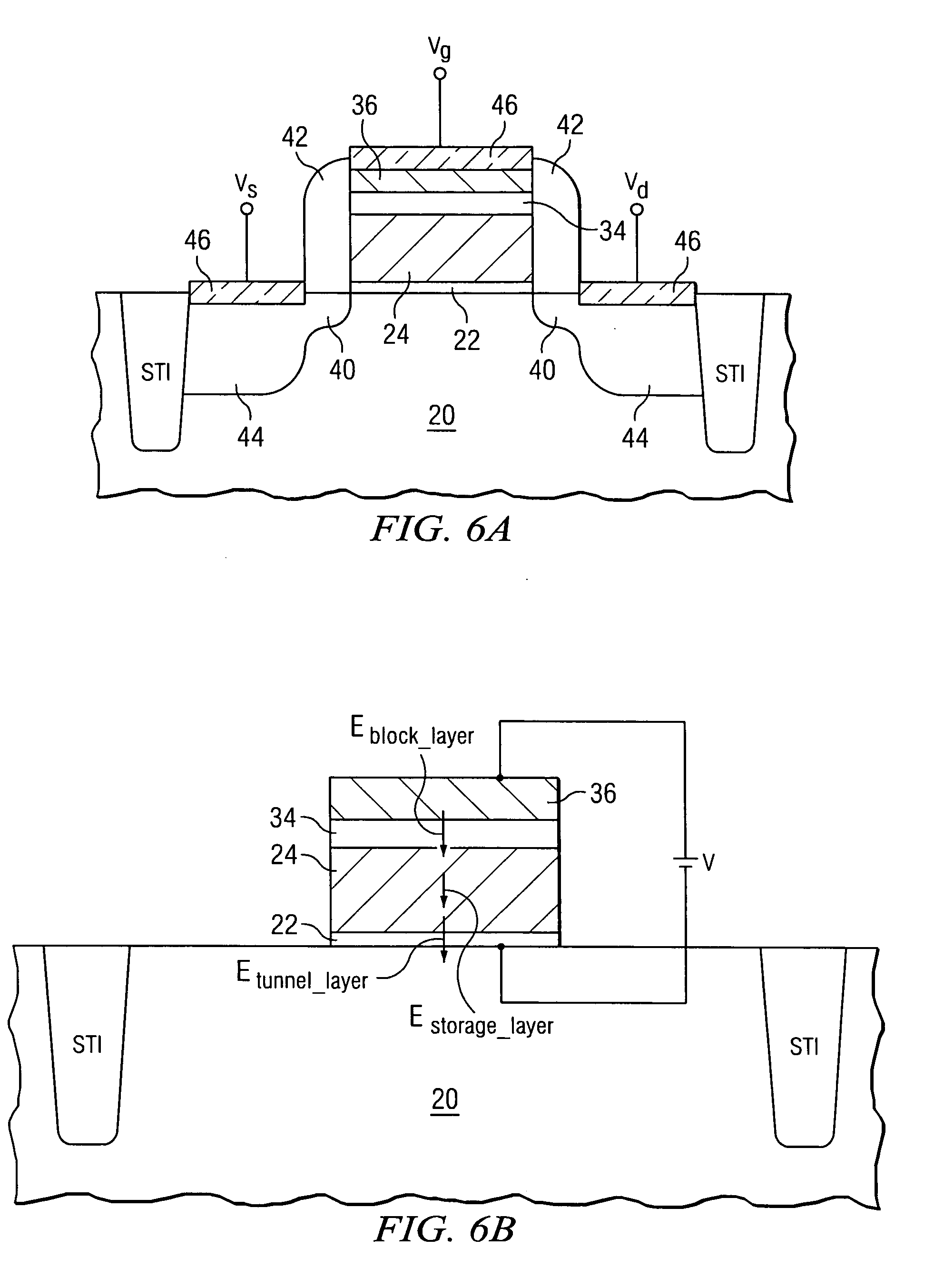
[0022]FIGS. 2A through 6A illustrate cross-sectional views of intermediate stages in the manufacture of a preferred embodiment. FIG. 2A illustrates shallow trench isolation (STI) regions formed ...


PUM


Abstract

A flash memory cell includes a substrate and a gate structure formed on the substrate. The gate structure includes a tunneling layer over the substrate, a storage layer over the tunneling layer, a blocking layer over the storage layer, and a gate electrode over the dielectric. The storage layer preferably has a conduction band lower than a conduction band of silicon. The blocking layer is preferably formed of a high-k dielectric material.

Description

TECHNICAL FIELD [0001]This invention relates generally to semiconductor devices, and more particularly to the structure and manufacturing methods of flash memory cells.BACKGROUND[0002]Flash memory has become increasingly popular in recent years. A typical flash memory comprises a memory array having a large number of memory cells arranged in blocks. One of the most commonly known flash memories is the one-transistor flash memory, wherein each of the memory cells is fabricated as a field-effect transistor having a control gate and a floating gate. The floating gate is capable of holding charges and is separated from source and drain regions contained in a substrate by a layer of thin oxide (tunneling oxide). Each of the memory cells can be electrically charged by injecting electrons from the drain region through the tunneling oxide layer onto the floating gate. The charges can be removed from the floating gate by tunneling the electrons to the substrate through the tunneling oxide la...

Claims


Application Information

Patent Timeline
IPC IPC(8): H01L29/06
CPCH01L29/517H01L29/792H01L29/66833
Inventor WANG, MING-TSONGONG, TONG-CHERNCHIN, ALBERTLAI, CHUN-HUNG
Owner TAIWAN SEMICON MFG CO LTD
Why Eureka
Try Eureka