
Intentional pocket shadowing to compensate for the effects of cross-diffusion in SRAMs

a technology of srams and pocket shadows, applied in the field of forming sram cells, can solve the problems of increased cross-diffusion and dose imbalance, increase the tendency toward device crowding, etc., and achieve the effect of reducing the width of the transistor and reducing the dose imbalan

Active Publication Date: 2007-12-13
TEXAS INSTR INC
View PDF4 Cites 34 Cited by
  • Summary
  • Abstract
  • Description
  • Claims
  • Application Information

AI Technical Summary

Benefits of technology

[0009]In addition, despite attempts to avoid pocket shadowing, as semiconductor features are aggressively reduced, pocket shadowing issues may increase, and associated disadvantageous effects resulting therefrom may become more prevalent as transistor widths and lengths are reduced. In general, the problems of pocket shadowing refer to dosage imbalances or the differences in the amount of dopant atoms received within certain areas (e.g., source / drain regions) as those areas are reduced in size. For example, shadowing tends to reduce the Vt of a transistor to less than its desired value. In addition, in situations where there is resist misalignment, a right transistor Vt, for example, may be altered more or less than a left transistor Vt, thereby disadvantageously creating transistor mismatch or other such imbalances. It can be appreciated that the effects of pocket shadowing may be even more noticeable in certain types of semiconductor devices, such as static random access memory (SRAM), for example, which incorporate multiple densely packed transistors that require matched electrical properties.
[0010]Semiconductor memories can, for example, be characterized as volatile random access memories (RAMs) or nonvolatile read only memories (ROMs), where RAMs can either be static (SRAM) or dynamic (DRAM) differing mainly in the manner by which they store a state of a bit. In SRAM, for example, each memory cell includes transistor-based circuitry that implements a bistable latch, which relies on transistor gain and positive (e.g., reinforcing) feedback so that it can only assume one of two possible states, namely on (state 1) or off (state 2).
[0011]The latch can only be programmed or induced to change from one state to the other through the application of a voltage or other external stimuli. This arrangement is desirable for a memory cell since a state written to the cell will be retained until the cell is reprogrammed. DRAMs on the other hand implement a capacitor that is either charged or discharged to store the on (state 1) or off (state 2) state of a cell. Capacitors discharge over time, however, and DRAMs must therefore be periodically ‘refreshed’. Also, a bistable latch can generally be switched between states much faster than the amount of time it takes to charge or discharge a capacitor. Accordingly, SRAMs are a desirable type of memory for certain types of applications.
[0012]SRAM is typically arranged as a matrix of memory cells fabricated in an integrated circuit chip, and address decoding in the chip allows access to each cell for read / write functions. SRAM memory cells use active feedback from cross-coupled inverters in the form of a latch to store or “latch” a bit of information. These SRAM memory cells are often arranged in rows so that blocks of data such as words or bytes can be written or read simultaneously. Standard SRAM memory cells have many variations. The basic CMOS SRAM cell generally includes two n-type (nMOS) pull-down or drive transistors and two p-type (pMOS) load transistors in a cross-coupled inverter configuration, with two additional nMOS select transistors added to make up a six-transistor cell (a 6T cell). Additionally, application specific SRAM cells can include an even greater number of transistors. Since a plurality of transistors are utilized in SRAM requiring matched electrical characteristics, and since pocket shadowing may become more prevalent as transistor widths are reduced, the adverse effects of pocket shadowing may present themselves to a great degree in SRAM, particularly as that type of memory is continually scaled down.
[0013]Accordingly, it would be desirable to obtain a technique that would allow symmetrically implanted active regions that compensate for the effects of cross-diffusion in highly scaled transistors, particularly where the transistors may be used in SRAM memory cells.SUMMARY OF THE INVENTION

Problems solved by technology

As previously indicated, scaling trends in the semiconductor industry are causing an increase tendency toward device crowding, resist misalignments, as well as in increased cross-diffusion and dose imbalances.

Method used


Image

  • Intentional pocket shadowing to compensate for the effects of cross-diffusion in SRAMs
  • Intentional pocket shadowing to compensate for the effects of cross-diffusion in SRAMs
  • Intentional pocket shadowing to compensate for the effects of cross-diffusion in SRAMs

Examples


Embodiment Construction

[0039]One or more aspects of the present invention are described with reference to the drawings, wherein like reference numerals are generally utilized to refer to like elements throughout, and wherein the various structures are not necessarily drawn to scale. In the following description, for purposes of explanation, numerous specific details are set forth in order to provide a thorough understanding of one or more aspects of the present invention. It may be evident, however, to one skilled in the art that one or more aspects of the present invention may be practiced with a lesser degree of these specific details. In other instances, known structures and devices are shown in block diagram form in order to facilitate describing one or more aspects of the present invention.

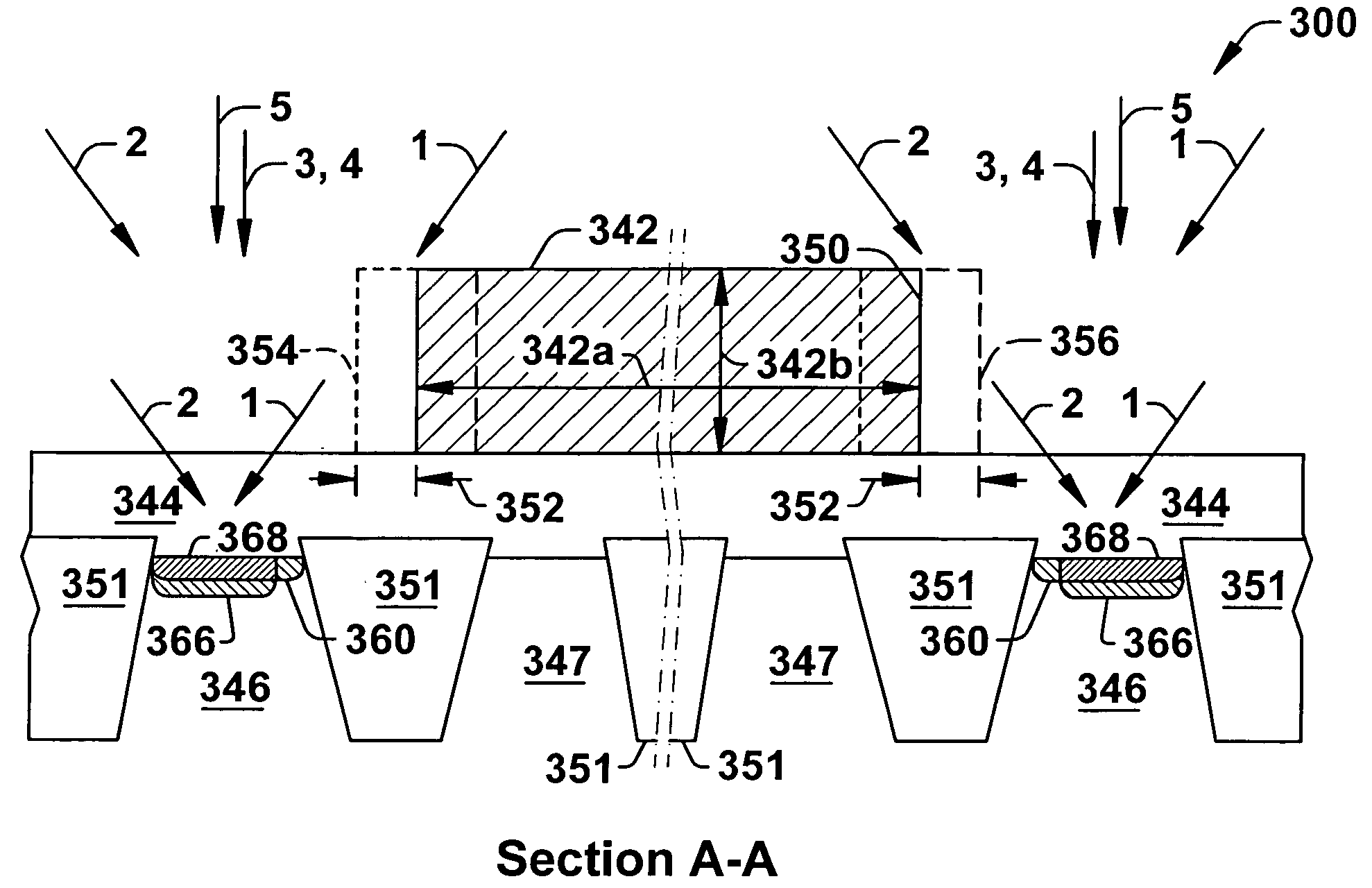
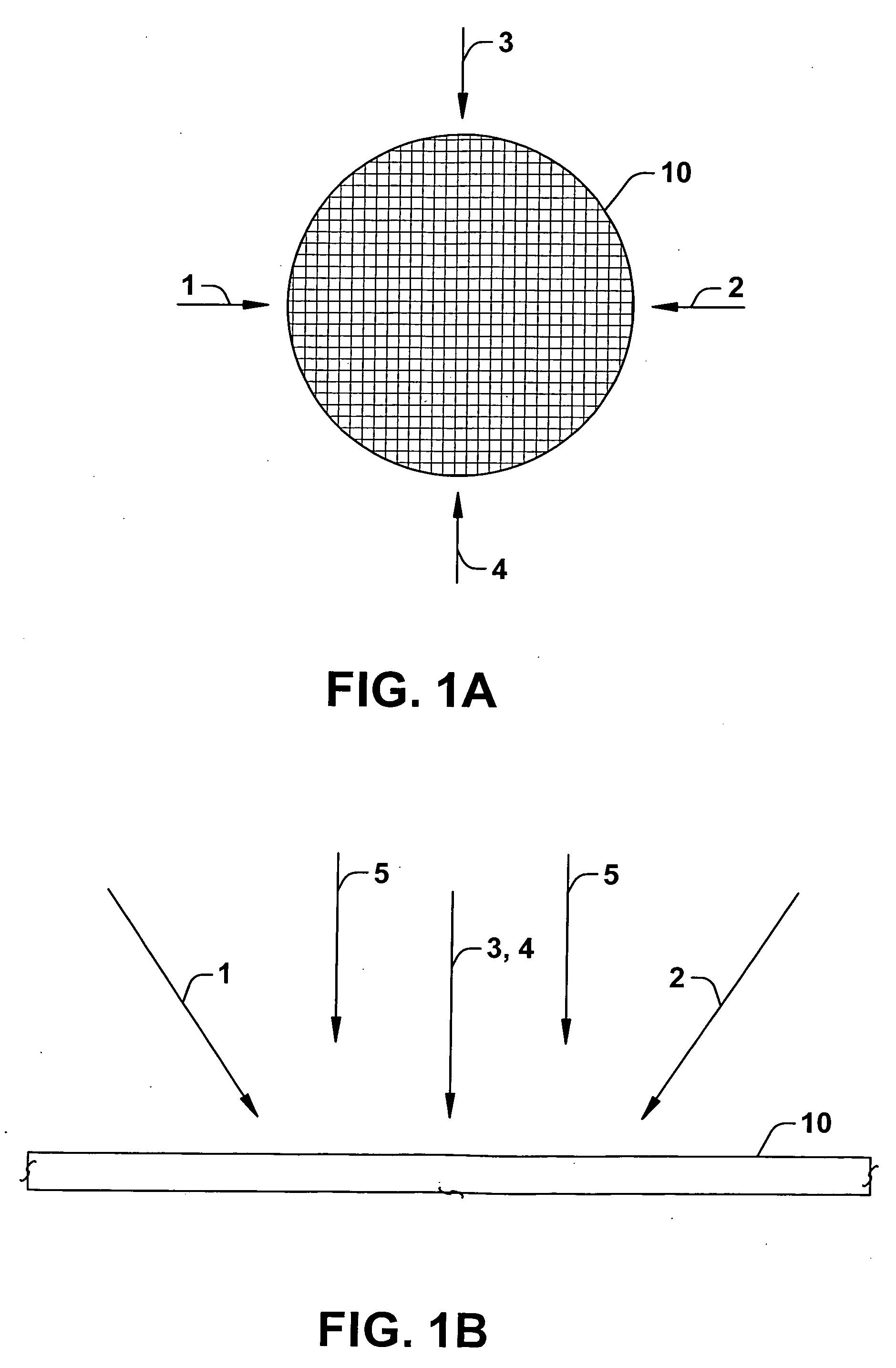
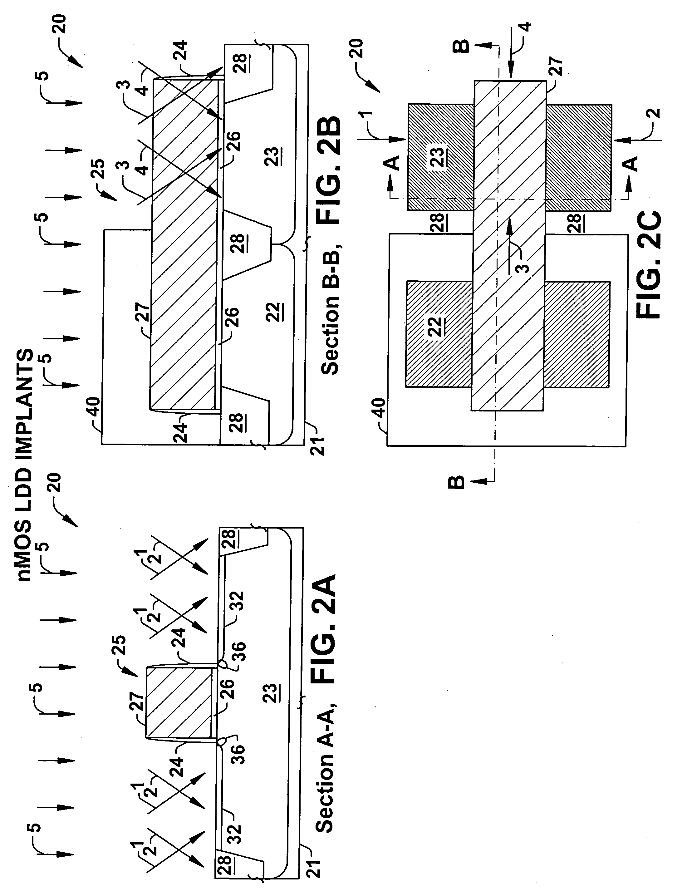
[0040]The present invention pertains to a method of providing an angled or pocket implant within the active regions of the cells of an SRAM memory array having symmetric shadowing in order to compensate for, counte...


PUM


Abstract

Methods are disclosed for forming an SRAM cell having symmetrically implanted active regions and reduced cross-diffusion therein. One method comprises patterning a resist layer overlying a semiconductor substrate to form resist structures about symmetrically located on opposite sides of active regions of the cell, implanting one or more dopant species using a first implant using the resist structures as an implant mask, rotating the semiconductor substrate relative to the first implant by about 180 degrees, and implanting one or more dopant species into the semiconductor substrate with a second implant using the resist structures as an implant mask. A method of performing a symmetric angle implant is also disclosed to provide reduced cross-diffusion within the cell, comprising patterning equally spaced resist structures on opposite sides of the active regions of the cell to equally shadow laterally opposed first and second angled implants.

Description

FIELD OF INVENTION[0001]The present invention relates generally to semiconductor processing, and more particularly to a method of forming an SRAM cell having symmetrically implanted active regions and reduced cross-diffusion by utilizing increased pocket shadowing during angled implantations to facilitate improved device matching characteristics, particularly in static random access memory (SRAM).BACKGROUND OF THE INVENTION[0002]Several trends presently exist in the semiconductor and electronics industry. Devices are continually being made smaller, faster and requiring less power. One reason for these trends is that more personal devices are being fabricated that are relatively small and portable, thereby relying on a battery as their primary supply. For example, cellular phones, personal computing devices, and personal sound systems are devices that are in great demand in the consumer market. In addition to being smaller and more portable, personal devices are also requiring increa...

Claims


Application Information

Patent Timeline
Patent Type & Authority Applications(United States)
IPC IPC(8): H01L21/338H01L21/425
CPCH01L27/1104H01L27/11H10B10/00H10B10/12
Inventor YOON, JONG SHIKCHATTERJEE, AMITAVASADRA, KAYVANTANG, SHAOPIN
Owner TEXAS INSTR INC
Features
  • Generate Ideas
  • Intellectual Property
  • Life Sciences
  • Materials
  • Tech Scout
  • Unparalleled Data Quality
  • Higher Quality Content
  • 60% Fewer Hallucinations
Learn More