Exposure Apparatus, Exposure Method, and Producing Method of Microdevice

a technology of micro-devices and exposure apparatuses, which is applied in the direction of photomechanical treatment, printing, instruments, etc., can solve the problems of inability to accurately expose, and varied optical properties of projection optical units, etc., to achieve high reliability, high quality, and high performance.

Inactive Publication Date: 2007-12-27
NIKON CORP
View PDF7 Cites 258 Cited by
  • Summary
  • Abstract
  • Description
  • Claims
  • Application Information

AI Technical Summary

Benefits of technology

[0012] According to the producing method of the microdevice of the third aspect of the invention, the exposing processing is carried out using the exposure apparatus of the first aspect of t...

Problems solved by technology

However, the column is slightly distorted and deformed in some cases when the mask stage or substrate stage is moved, and there is a problem that the optical property (imaging property) of the projection optical unit is varied and precise exposing processing can not be carried out.
Especially in the case of a structure in which the plurality of projection optical unit are supported using different support bodies, relative positions of the plurality of projection optical units are varied and precise exposing processing can not be carried out.
Since the mask stage and substrate stage move in the same direction during the scanning and exposing operation, ...

Method used


Image

  • Exposure Apparatus, Exposure Method, and Producing Method of Microdevice
  • Exposure Apparatus, Exposure Method, and Producing Method of Microdevice
  • Exposure Apparatus, Exposure Method, and Producing Method of Microdevice

Examples


first embodiment

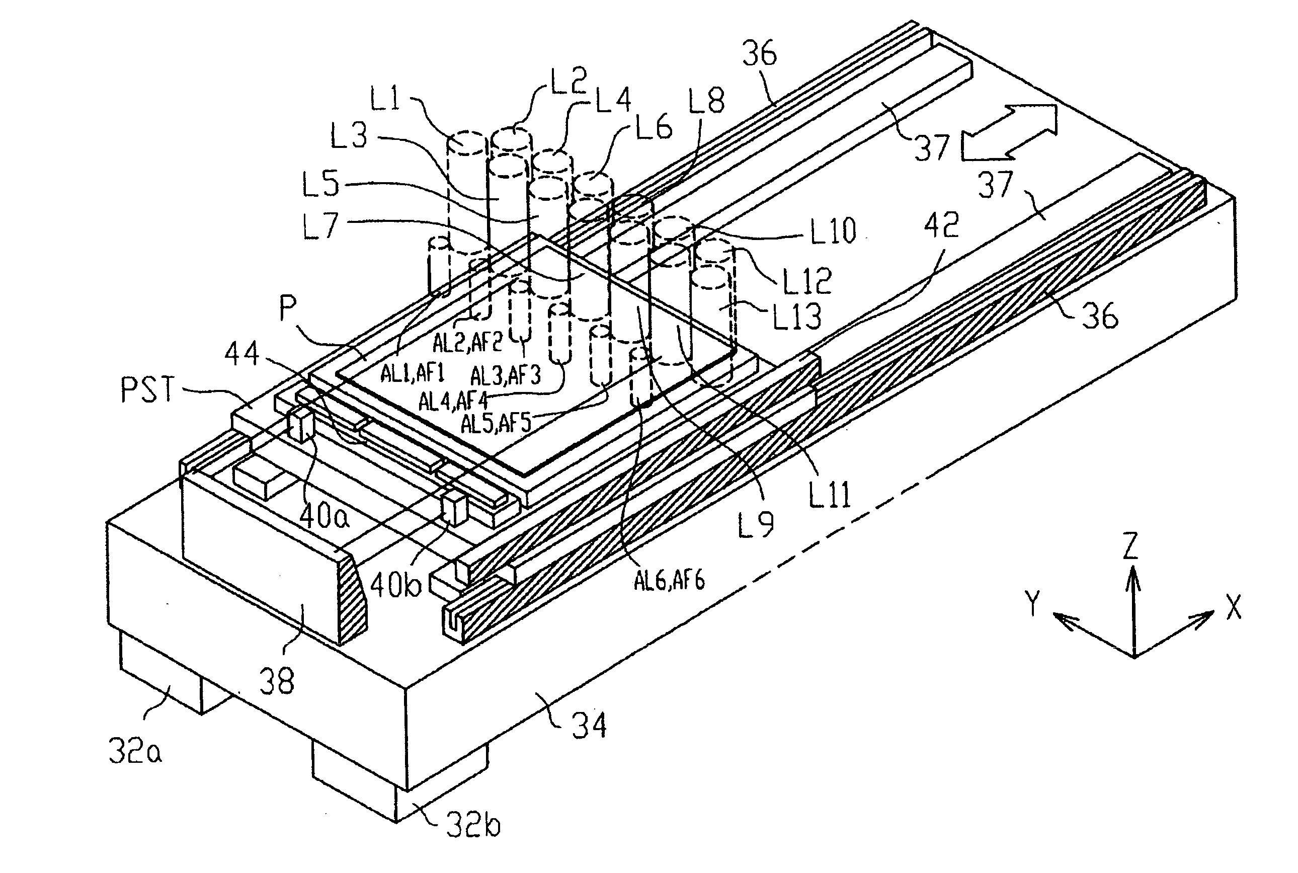
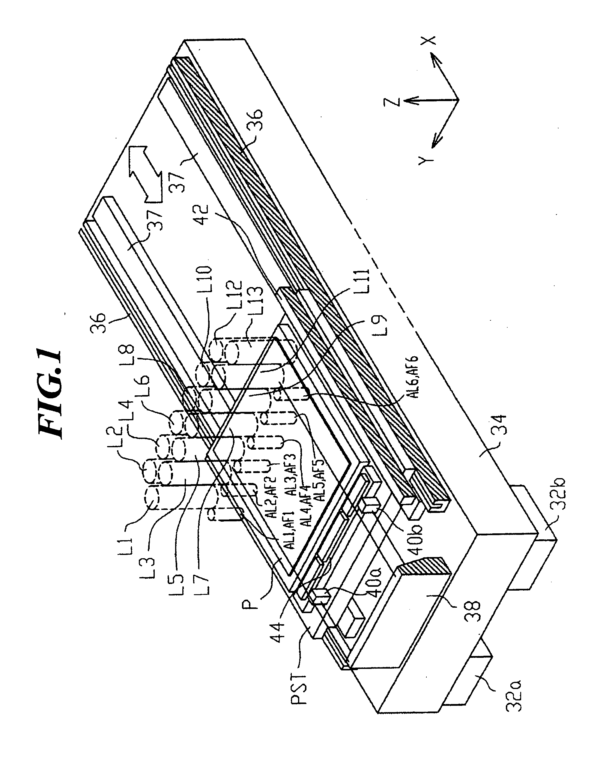
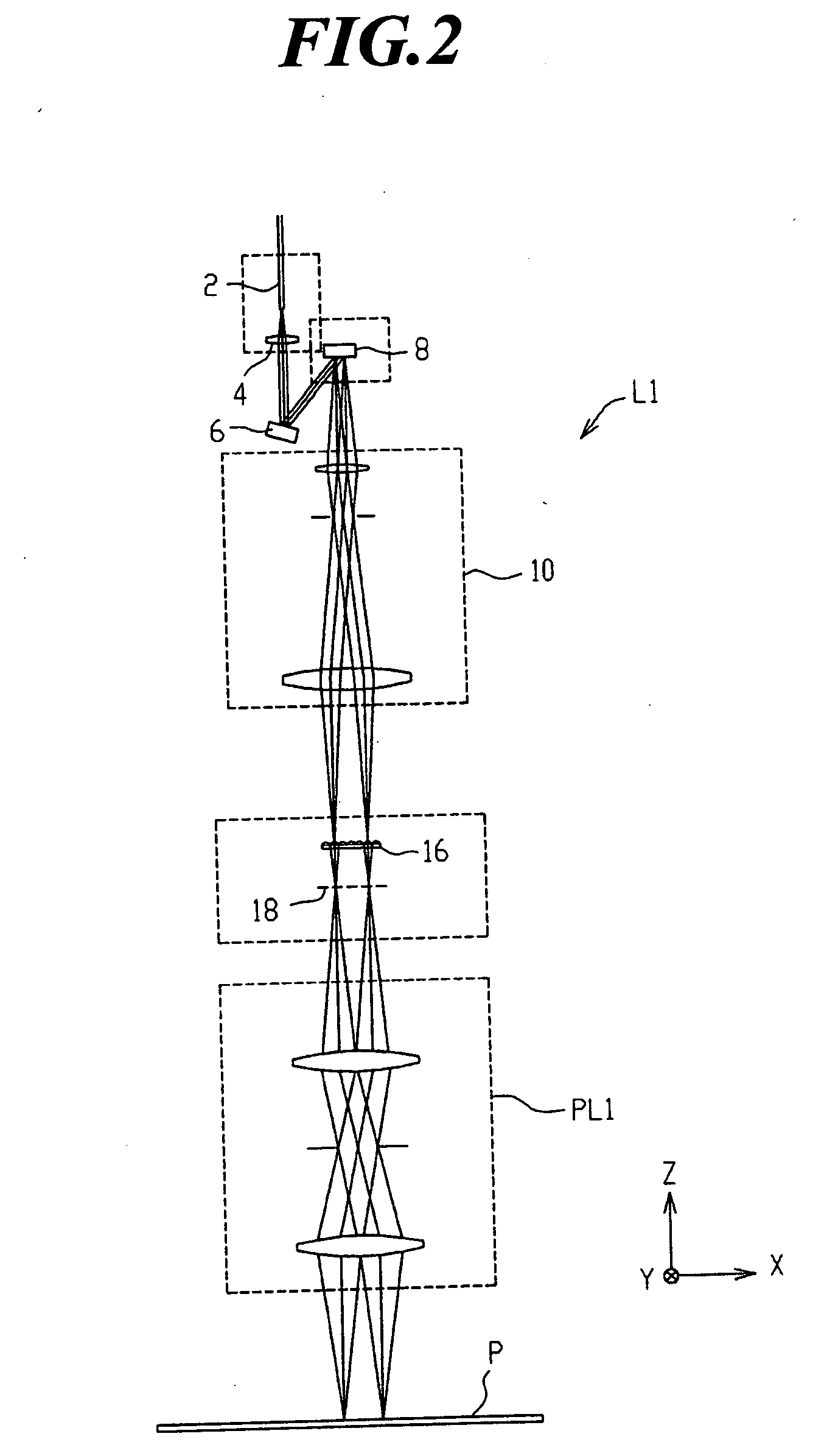
[0063] A first embodiment of the present invention will be explained below with reference the drawings. FIG. 1 is a schematic perspective view of a structure of a scanning type exposure apparatus of the first embodiment of the invention. In this embodiment, a scanning type projection exposure apparatus employs a step-and-scanning method in which a pattern of a liquid crystal display element or the like is transferred onto a plate P while relatively moving, with respect to a plurality of exposure optical systems L1 to L13, a plate P as a photosensitive substrate on which a photosensitive material (resist) is applied.

[0064] In the following explanation, a rectangular coordinate system shown in FIG. 1 is set, and a positional relation of various members will be explained with reference to the XYZ rectangular coordinate system. In the XYZ rectangular coordinate system, the X-axis and Y-axis are in parallel to the plate P, and the Z-axis intersects with the plate P. In the XYZ coordinat...

second embodiment

[0143] Next, a second embodiment of the invention will be explained with reference to the drawings. FIG. 31 is a schematic diagram showing a structure of an exposure apparatus of the second embodiment of the invention. FIG. 32 is a schematic perspective view. In FIGS. 31 and 32, an exposure apparatus EX includes a mask stage MST for supporting a mask M formed with a pattern, a substrate stage (plate stage) PST for supporting a photosensitive substrate (plate) P having an outer diameter greater than 500 mm, an illumination optical system IL for illuminating the mask M supported by the mask stage MST with the exposure light L, a projection optical system PL for projecting an image of a pattern of the mask M illuminated by the exposure light L onto the photosensitive substrate P supported by the substrate stage PST, a column 100 for supporting the projection optical system PL through a surface plate 101, and a control device CONT2 for controlling action concerning the exposing processi...


PUM


Abstract

An exposure apparatus for exposure-transferring an image of a pattern projected through an optical system having a plurality of optical units L1 to L13 onto an object P, comprises a correcting device which corrects a position of at least one of a plurality of images to be projected onto the object P by the plurality of optical units L1 to L13 so that displacements of the optical units L1 to L13 are compensated.

Description

TECHNICAL FIELD [0001] The present invention relates to an exposure apparatus in which an image of a pattern is projected by a projection optical system onto an object such as a photosensitive substrate and the image is exposure-transferred on the object. The invention also relates to an exposure method and a producing method of a microdevice using the exposure apparatus. BACKGROUND ART [0002] A flat-panel display element such as a liquid crystal display device is produced by a so-called photolithography technique in which a pattern formed on a mask is transferred onto a photosensitive substrate. An exposure apparatus used in the photolithography step includes a mask stage for supporting a mask, and a substrate stage for supporting a substrate. The exposure apparatus transfers the pattern of the mask onto the substrate through a projection optical system while sequentially moving the mask stage and the substrate stage. When the liquid crystal display device of the display elements i...

Claims


Application Information

Patent Timeline
IPC IPC(8): G03B27/42
CPCG03F7/70275G03F7/70791G03F7/70308G03F9/7003
Inventor KATO, MASAKISHIMIZU, KENJITOGUCHI, MANABUWATANABE, TOMOYUKI
Owner NIKON CORP
Why Eureka
Try Eureka