Partial Page Fail Bit Detection in Flash Memory Devices

a flash memory device and fail bit technology, applied in error detection/correction, digital storage, instruments, etc., can solve the problems of consuming substantial time and power, cells are slower to program or erase, and cannot be programmed or erased in any way, so as to improve the efficiency of error correction coding, modest error correction coding capacity, and enhanced scaling of flash memory page sizes

Active Publication Date: 2008-01-03
SANDISK TECH LLC
View PDF17 Cites 99 Cited by
  • Summary
  • Abstract
  • Description
  • Claims
  • Application Information

AI Technical Summary

Benefits of technology

[0038]It is therefore an object of this invention to provide flash memory circuitry for verifying programmed and erased conditions in a manner that improves the efficiency of error correction coding.
[0039]It is a further object of this invention to provide such circuitry that enables earlier termination of programming and erase operations.
[0040]It is a further object of this invention to provide such circuitry that enables enhanced scaling of flash memory page sizes to include additional sectors, with modest error correction coding capacity.
[0041]It is a further object of this invention to provide such circuitry that is more tolerable of slow-to-program or defective memory cells within a given page, thus improving the manufacturing yield for a given technology and manufacturing process, and without reducing device reliability.

Problems solved by technology

Of course, a tradeoff exists between the yield savings and the cost of providing additional memory cells to store the code bits (i.e., the code “rate”).
Indeed, considering that the programming and erasing of flash memory cells are typically performed by the application of a sequence of pulses of the appropriate voltages, and also considering that the pulse sequences consume substantial time and power, many flash memories now include verification operations during the programming or erasing operations themselves.
As is well known in this art, some memory cells are slower to program or erase than others, because of manufacturing variations among those cells, because those cells were previously erased to a lower threshold voltage than others, because of uneven wear among the cells within a page, or the like.
And, of course, some cells cannot be programmed or erased whatsoever, because of a manufacturing defect.
However, the counting of failed bits may not be performed until the terminal number of programming cycles is reached, because the fail bit count can be quite time consuming, if performed in every verify operation.
In other, typically more advanced, flash memory applications, the counting of failed bits is not performed until a certain number of program-and-verify loops have been completed, because it is unlikely that the ignore bit limit will be met at that point.
As evident from the above description, programming of flash memory cells can be a time consuming process, especially when verify operations are involved in the iterative programming of a page.

Method used


Image

  • Partial Page Fail Bit Detection in Flash Memory Devices
  • Partial Page Fail Bit Detection in Flash Memory Devices
  • Partial Page Fail Bit Detection in Flash Memory Devices

Examples


Embodiment Construction

[0050]This invention will be described in connection with its preferred embodiment, namely as implemented into a flash memory device, for example a flash memory device including multi-level programming cells (MLC) arranged in NAND fashion. However, it is contemplated that this invention may also be beneficial if applied in other types of memory architectures and devices. It is contemplated that such other alternative realizations are within the scope of this invention. Accordingly, it is to be understood that the following description is provided by way of example only, and is not intended to limit the true scope of this invention as claimed.

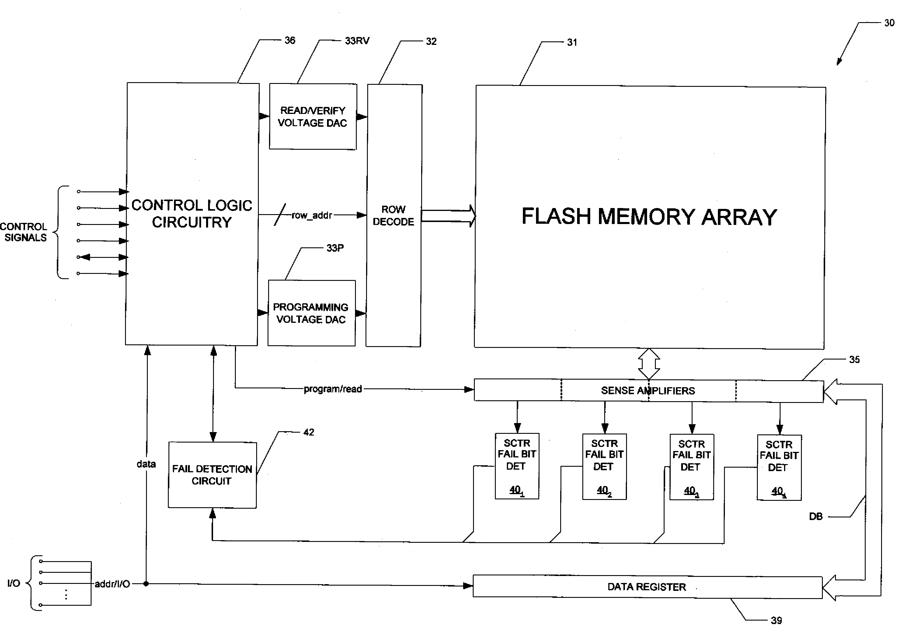
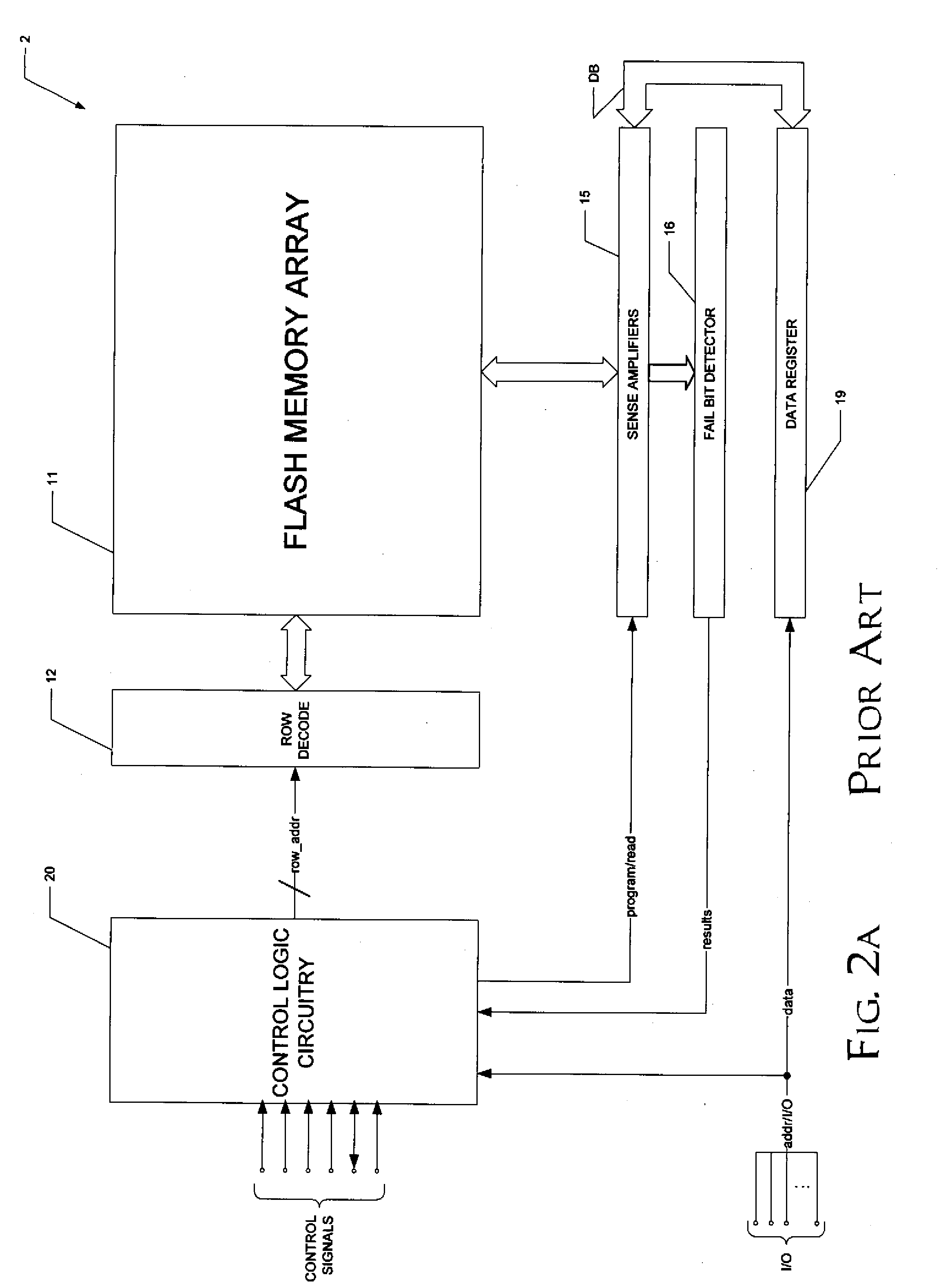
[0051]FIG. 4 illustrates an example of the architecture of flash memory device 30 according to the preferred embodiments of the invention. The construction of flash memory device 30 is similar, in many respects, as that of conventional flash memory devices such described in FIG. 2a. As such, flash memory device 30 includes flash memory array 31 ...


PUM


Abstract

A flash memory device, and a method of operating the same, is disclosed. The array of the flash memory device is arranged in pages of memory cells, each page having memory cells associated into groups of memory cells within the page for purposes of fail bit detection in program verification. For example, these groups may correspond to sectors within the page. In a programming operation, the verify process determines whether each group of memory cells within the page has fewer than a selected ignore bit limit for the sector. If not, additional programming is required for the insufficiently programmed cells in the page. By applying a fail bit detection threshold for each of multiple groups within the page, the efficiency of error correction coding in the flash memory is improved. A similar verify and fail bit detection approach may be used in erase and soft programming operations.

Description

CROSS-REFERENCE TO RELATED APPLICATIONS[0001]This application is related to copending application Ser. No. ______, (Attorney Docket No. SDK0766.000US), entitled “Method of Partial Page Fail Bit Detection in Flash Memory Devices”, which is commonly assigned with, and has the same filing date as, this application.STATEMENT REGARDING FEDERALLY SPONSORED RESEARCH OR DEVELOPMENT[0002]Not applicable.BACKGROUND OF THE INVENTION[0003]This invention is in the field of solid-state non-volatile memory, and is more specifically directed to the detection of failed memory cells in such memory.[0004]As well known in the art, “flash” memories are electrically-erasable and rewritable semiconductor memory devices that can be erased at once (in a “flash”) on a chip-wide basis, or in smaller units referred to as blocks. As such, flash memory has become especially popular for applications in which non-volatility (i.e., data retention after removal of power) of the stored data is essential, and in which ...

Claims


Application Information

Patent Timeline
Patent Type & Authority Applications(United States)
IPC IPC(8): G11C16/04
CPCG06F11/1068G11C16/349G11C16/10
Inventor HEMINK, GERRIT JAN
Owner SANDISK TECH LLC
Why Eureka
Try Eureka