Eureka AIR delivers breakthrough ideas for toughest innovation challenges, trusted by R&D personnel around the world.

Method of manufacturing semiconductor device

Inactive Publication Date: 2008-01-03
SEMICON ENERGY LAB CO LTD
View PDF27 Cites 15 Cited by
  • Summary
  • Abstract
  • Description
  • Claims
  • Application Information

AI Technical Summary

Benefits of technology

[0011]In addition, since a plastic substrate is flexible, alignment in pattern formation is less precise than a case of using a glass substrate. Therefore, yields may be decreased.
[0012]In view of the foregoing, the present invention provides a method of manufacturing a semiconductor device which is manufactured by peeling an element group which is formed over a glass substrate and transferring the element group to a plastic substrate. In specific, a liquid repellent film is formed over a substrate, a base film is formed over the liquid repellent film, an element group is formed over the base film, and the element group which is formed is peeled off. Since adhesion between the liquid repellent film and the base film is low, the peeling is easily conducted. Further, a region other than a region in which the element group to be peeled is formed is not provided with the liquid repellent film (a non-liquid repellent region), whereby undesired peeling can be prevented. Formation of a liquid repellent region and a non-liquid repellent region is conducted by light exposure.
[0037]According to the present invention, the possibility that an element group is influenced mechanically and electrostatically and damaged in peeling and transferring steps can be reduced. Accordingly, a TFT can be manufactured over a flexible substrate with high yield.
[0038]In the present invention, a TFT is manufactured over a substrate having heat resistance; therefore, alignment in pattern formation can be precise compared to a case in which a TFT is formed directly over a plastic substrate. Further, a TFT can be manufactured over a flexible substrate with high yield, without significant restriction on apparatuses, conditions, and the like.
[0039]Furthermore, by using the present invention, a semiconductor device itself can be thin compared with a conventional manufacturing method, in which a TFT is transferred to a plastic substrate.

Problems solved by technology

However, it is not preferable that a TFT is manufactured over a glass substrate and then transferred to a plastic substrate through a peeling step and a transferring step, because the TFT and a peripheral element may be influenced mechanically and damaged in a step of peeling off the TFT from the glass substrate, or transferring the TFT, which is peeled, to the plastic substrate.
Further, there is a possibility that static electricity is generated in these steps and the generated static electricity damages the TFT and the peripheral element, which may lead to significant reduction in yields.
On the other hand, in a case of manufacturing a TFT over a plastic substrate without peeling and transferring steps, there are much restriction on apparatuses, conditions, and the like, compared with a case of manufacturing a TFT over a glass substrate and then transferring the TFT to the plastic substrate through the peeling and transferring steps.
In addition, since a plastic substrate is flexible, alignment in pattern formation is less precise than a case of using a glass substrate.

Method used


Image

  • Method of manufacturing semiconductor device
  • Method of manufacturing semiconductor device
  • Method of manufacturing semiconductor device

Examples


embodiment mode 1

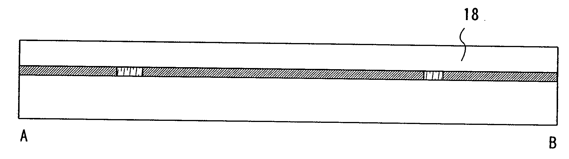
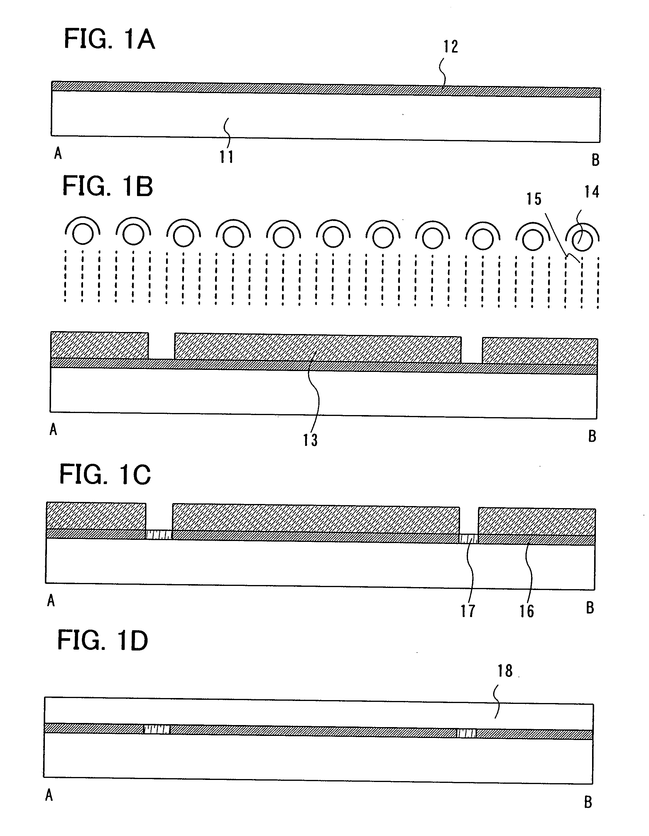
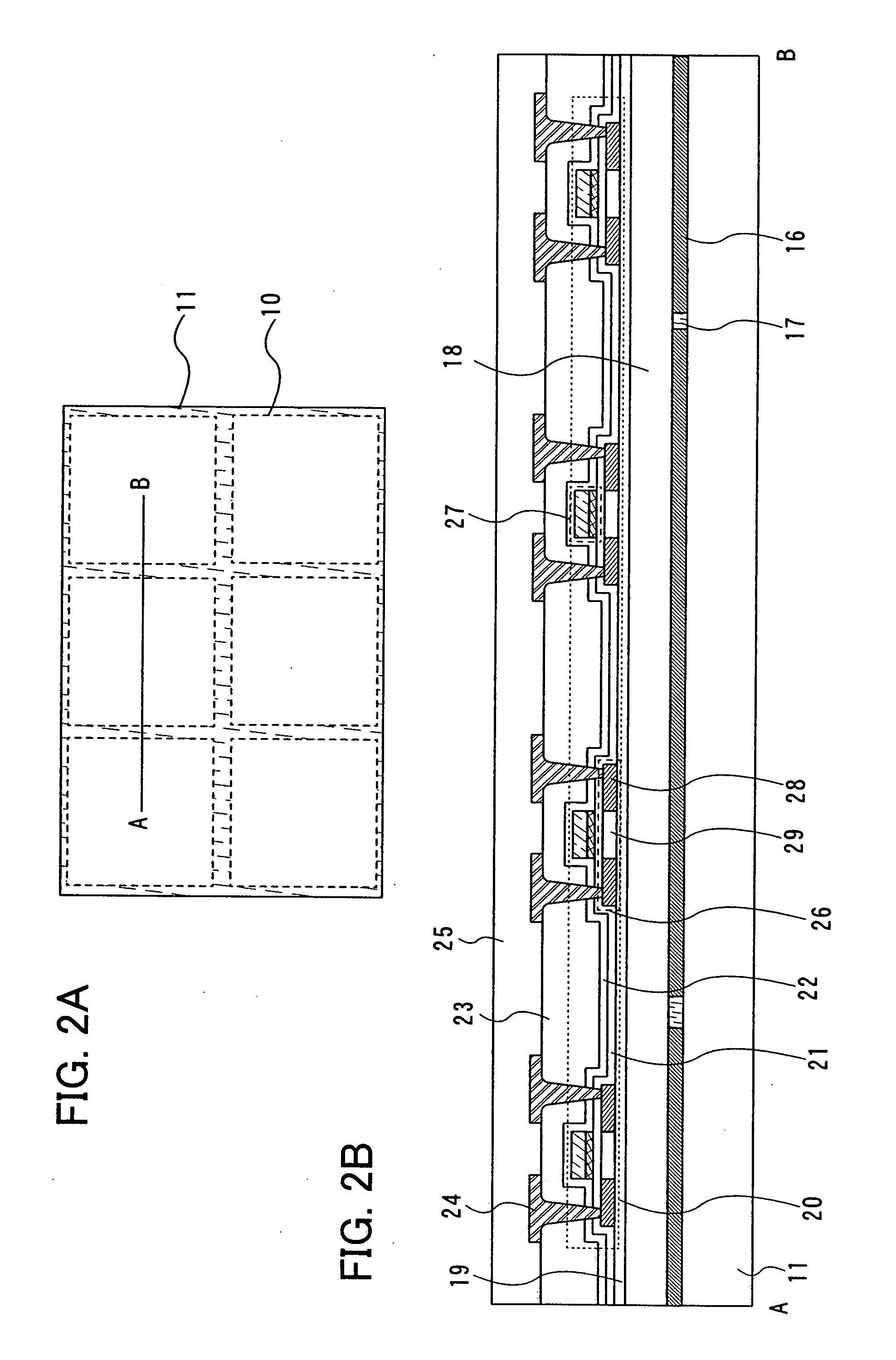
[0054]A manufacturing method of a semiconductor device of the present invention is described with reference to FIGS. 1A to 4B. A case in which six semiconductor devices are manufactured over a substrate is described below. In each of FIGS. 2A, 3A, and 4A, a region in which one semiconductor device is provided corresponds to a region 10 surrounded by a dotted line. FIGS. 2B, 3B, and 4B correspond to cross-sectional views taken along lines A-B in FIGS. 2A, 3A, and 4A, respectively. In addition, cross-sectional views in FIGS. 1A to 1D correspond to cross-sectional views taken along lines A-B in FIGS. 2A, 3A, and 4A.

[0055]First, a liquid repellent film 12 is formed over a substrate 11 as a liquid repellent self-assembled monolayer (see FIG. 1A). The liquid repellent film 12 may be formed using a silane coupling agent having a fluoroalkyl group (fluoroalkylsilane, hereinafter referred to as FAS). The substrate which is heated and FAS are confined so as to form a FAS self-assembled monola...

embodiment mode 2

[0080]In a method of manufacturing a semiconductor device of the present invention, FAS can be decomposed by back surface light exposure. The use of back surface light exposure can omit a removing step of a mask. In this embodiment mode, a substrate with a light-transmitting property (hereinafter, referred to as a light-transmitting substrate) is used so that back surface light exposure can be conducted. A substrate which transmits light that is used in the back surface light exposure is used as the light-transmitting substrate. A description is made below with reference to FIGS. 2A to 5D. Note that the same layers are denoted by the same reference numerals in different embodiment modes.

[0081]First, the mask which blocks light is formed over a light-transmitting substrate 11a. As the light-transmitting substrate 11a, a quartz substrate may be used, for example. A material for the mask 13 is not specifically limited and is acceptable as long as the material can block the light 15 whi...

embodiment mode 3

[0090]In a method of manufacturing a semiconductor device of the present invention, FAS can be decomposed by back surface light exposure as described in Embodiment Mode 2. Note that, since it is necessary to use light which is in a wavelength range with which the light can pass through a light-transmitting substrate and a liquid repellent film can be decomposed, there is a possibility that the light in a wavelength range needed for decomposition of the liquid repellent film does not reach the liquid repellent film, depending on a combination of the light-transmitting substrate and the liquid repellent film. A case in which a glass substrate is used as the light-transmitting substrate and FAS is used for the liquid repellent film can be given as an example of such a situation. A glass substrate does not transmit light in a wavelength range of less than or equal to 300 nm, whereas FAS needs light in a wavelength of less than or equal to 200 nm to be decomposed; therefore, a liquid rep...


PUM


Abstract

A method of manufacturing a thin TFT over a flexible substrate is provided. In formation of a TFT on a surface of a substrate having heat resistance, a liquid repellent film is formed selectively on a surface of the substrate, and an organic film is formed thereover. An element such as a TFT is formed over the organic film. Since the liquid repellent film is formed over the substrate, adhesion between the substrate and the organic film is low; therefore, the element which is formed can be peeled off from the substrate easily. Further, since the element is not transferred to another substrate, a semiconductor device which is thinner than conventional ones can be manufactured. In order to form the liquid repellent film selectively, light exposure of a front surface or a back surface of the substrate provided with a mask, a droplet discharging method, or the like is used.

Description

BACKGROUND OF THE INVENTION[0001]1. Field of the Invention[0002]The present invention relates to a method of manufacturing a semiconductor device. In particular, the present invention relates to a method of manufacturing a semiconductor device which is formed over a flexible substrate.[0003]2. Description of the Related Art[0004]In recent years, a technology for semiconductor devices having thin film transistors (hereinafter referred to as TFTs) including semiconductor films formed over insulating substrates has been developed extensively. TFTs are widely used as switching element for operation of a display element, an IC tag, and the like.[0005]A glass substrate, a quartz substrate, and the like have been heretofore used as a substrate for forming TFTs. These substrates have disadvantages in that they are easily broken and are heavy. Therefore, in recent years, a flexible substrate attracts attention in particular. A flexible substrate is thin, light weight, and bendable; therefore...

Claims


Application Information

Patent Timeline
IPC IPC(8): H01L21/84
CPCH01L27/1266H01L27/1255H01L29/78603
Inventor JINBO, YASUHIRO
Owner SEMICON ENERGY LAB CO LTD
Why Eureka
Eureka Blog
Learn More