Charge Domain Filter Device

a filter device and charge domain technology, applied in the field of filter devices, can solve the problems of difficult to achieve higher-order filtering without, the low-pass filter circuit of the charge domain sinc filter circuit in the related art fails to achieve superior characteristics as low-pass filter, and the application range is still very limited. to achieve the effect of efficient passing the low-range componen

Inactive Publication Date: 2008-01-10
SONY CORP
View PDF12 Cites 20 Cited by
  • Summary
  • Abstract
  • Description
  • Claims
  • Application Information

AI Technical Summary

Benefits of technology

[0028] According to the embodiments of the present invention described above, a new and improved charge domain filter device, capable of e

Problems solved by technology

However, the charge domain SINC filter circuits in the related art fail to achieve superior characteristics as low pass filters.
Higher-order filtering is difficult to be achieved without altering the sampling rate in a charge domain filter circuit.
While the low-range component characteristics are improved in the method disclosed in Nonpatent Reference literature 3 with the frequency characteristics raised to the second power of the SINC, its application range is still very limited since, unlike an FIR (finite impulse response) filter, it doe

Method used


Image

  • Charge Domain Filter Device
  • Charge Domain Filter Device
  • Charge Domain Filter Device

Examples


first embodiment

[0049] First, the charge domain filter circuit achieved in the first embodiment of the present invention is described.

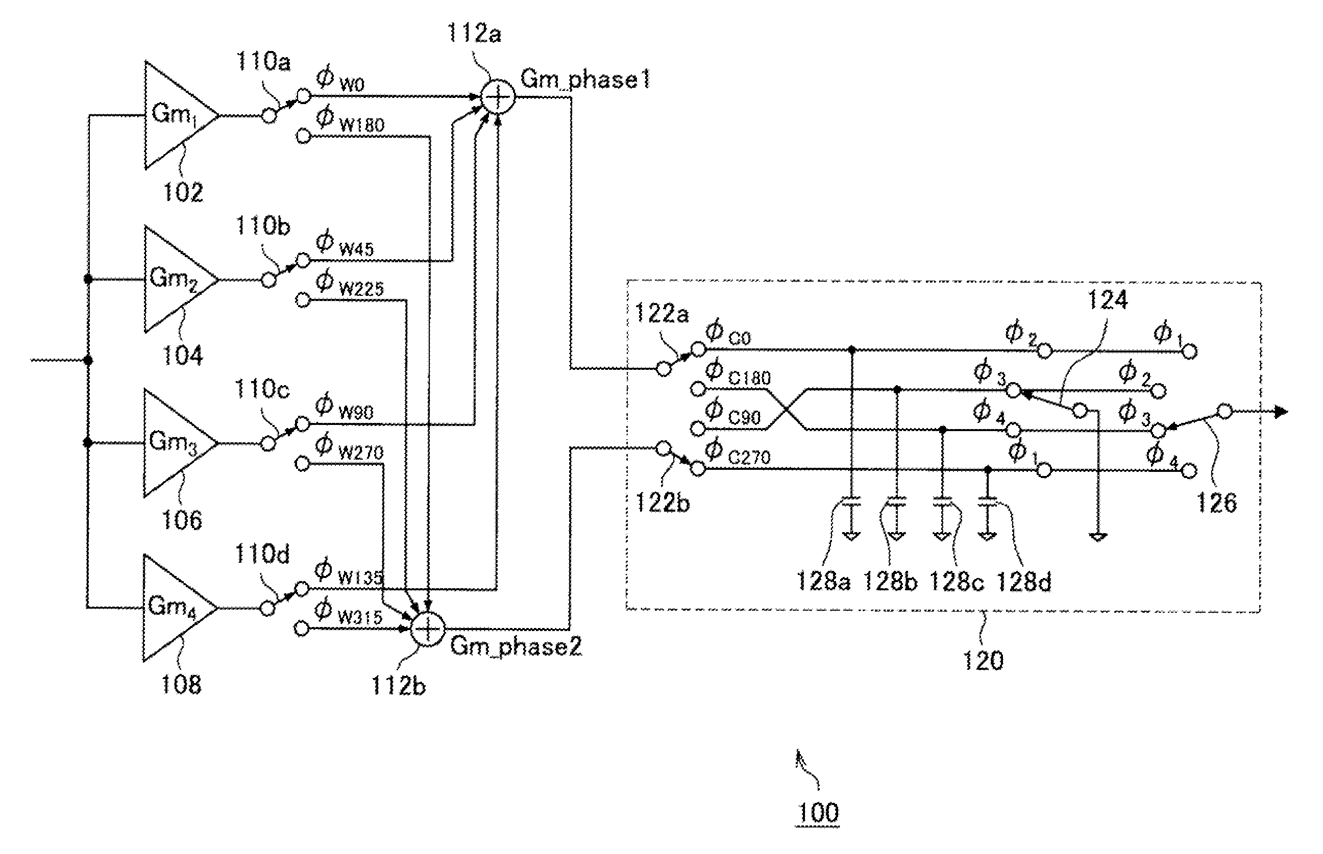
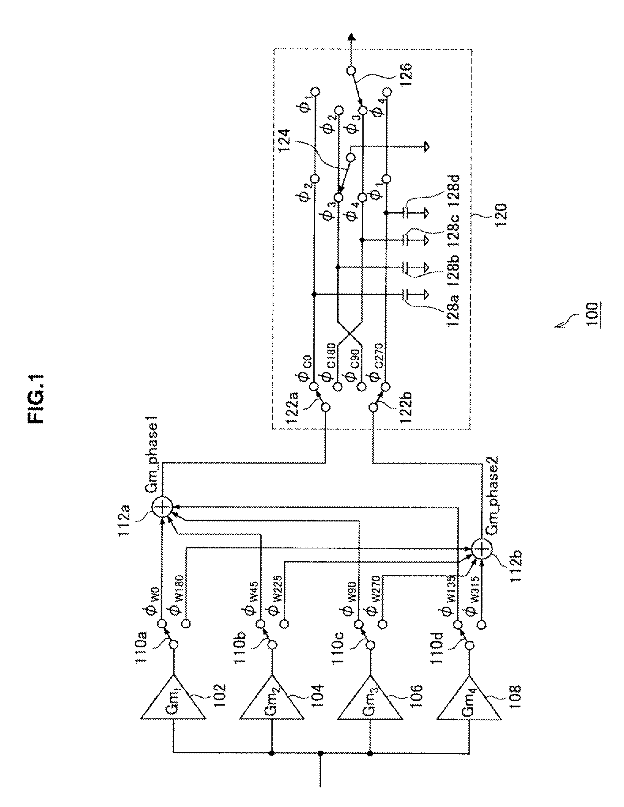
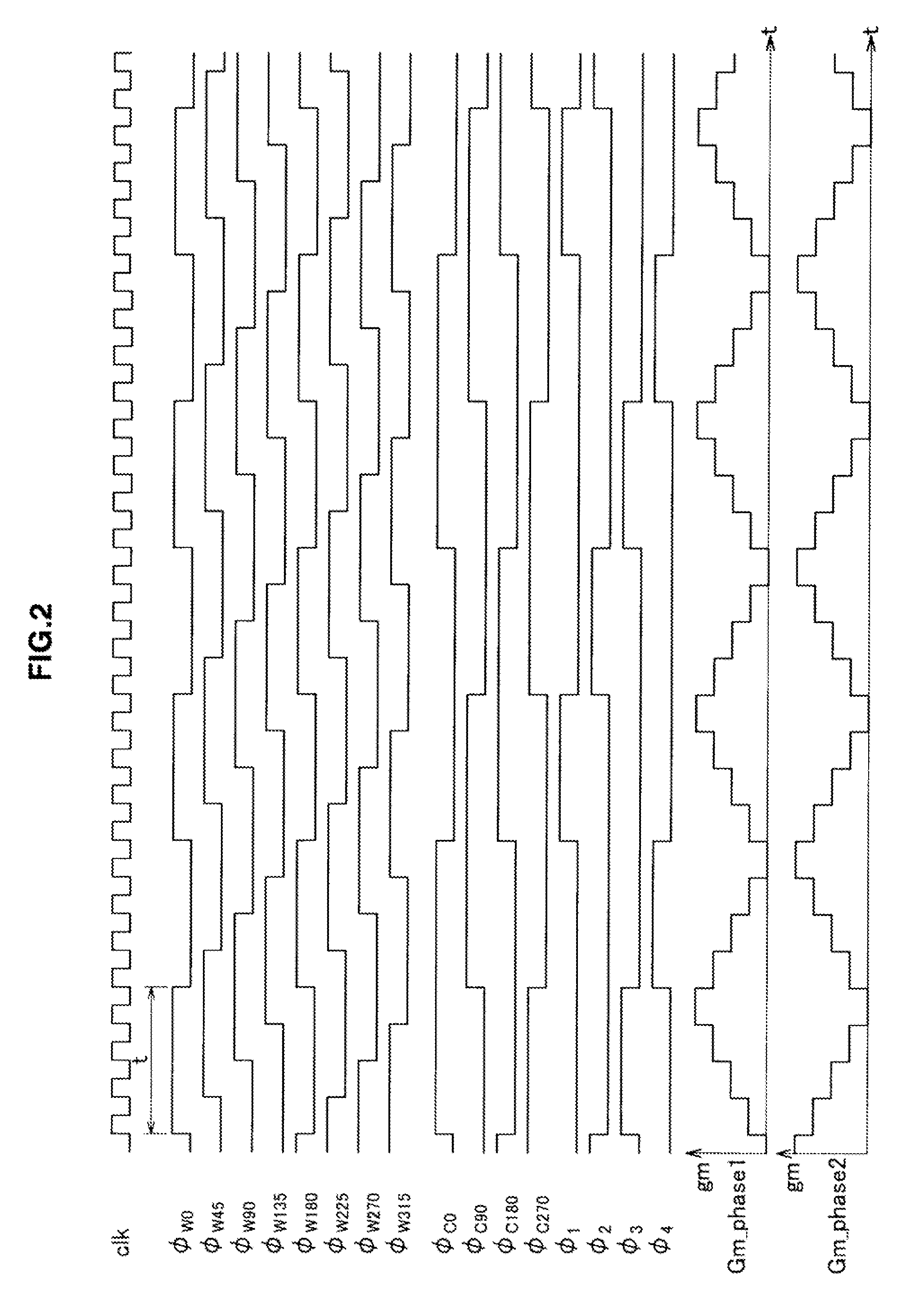
[0050]FIG. 1 shows the charge domain filter circuit achieved in the first embodiment of the present invention. As shown in FIG. 1 the charge domain filter circuit 100 in the first embodiment of the present invention includes transconductors 102, 104, 106 and 108, switches 110a, 110b, 110c and 110d, adders 112a and 112b and a SINC filter circuit 120.

[0051] The SINC filter circuit 120 includes first switches 122a and 122b, a second switch 124, a third switch 126 and capacitors 128a, 128b, 128c and 128d.

[0052] The transconductors 102, 104, 106 and 108 each output a current in proportion to the voltage of an input signal. While four transconductors are used to constitute the charge domain filter circuit in the embodiment, the number of transconductors in a charge domain filter circuit embodying the present invention is not limited to four. In addition, the transconduc...

second embodiment

[0103] An explanation is given above in reference to the first embodiment of the present invention on a charge domain filter circuit, the frequency characteristics of which can be adjusted freely by controlling the timing with which the currents output from the transconductors are added up. Now, in reference to the second embodiment of the present invention, a charge domain filter circuit, the frequency characteristics of which can be adjusted freely by controlling the timing with which the electrical charges output from SINC filter circuits are added up, is described.

[0104]FIG. 7 illustrates the charge domain filter circuit achieved in the second embodiment of the present invention. The following is an explanation of the charge domain filter circuit achieved in the second embodiment of the present invention, given in reference to FIG. 7.

[0105] As shown in FIG. 7, a charge domain filter circuit 200 in the second embodiment of the present invention includes transconductors 202, 204...

application example 1

[0147]FIGS. 9A and 9B illustrate an example of impulse response. When the pulse width of the clocks used to charge the capacitors includes three clock and the charge domain filter circuit includes five transconductors, with three transconductors among them assuming a transconductance twice that of the remaining two, as shown in FIG. 9A, the impulse response shown in FIG. 9B is obtained. The impulse response shown in FIG. 9B is identical to that shown in FIG. 5B. Accordingly, assuming that the sampling cycle t is equal to 1 ns, the frequency characteristics achieved under these circumstances, too, are as indicated by the graph in FIG. 6.


PUM


Abstract

There is provided a charge domain filter device including a plurality of transconductors each of which converts an input voltage to a current and outputs the current and a filter unit that filters output signals from said plurality of transconductors by repeatedly charging and discharging a plurality of capacitors, wherein an impulse response of the charge domain filter device is obtained through convolution of a first impulse corresponding to a charge time length over which said capacitors are charged and a second impulse corresponding to each of said plurality of transconductors.

Description

CROSS REFERENCE TO RELATED APPLICATION [0001] The present invention contains subject matter related to Japanese Patent Application No. JP 2006-187057 filed in the Japan Patent Office on Jul. 6, 2006, the entire contents of which being incorporated herein by reference. BACKGROUND OF THE INVENTION [0002] 1. Field of the Invention [0003] The present invention relates to a filter device designed by charge domain operations (hereinafter, called a charge domain filter device). [0004] 2. Description of the Related Art [0005] An SoC (system-on-chip) used in wireless communication, which is achieved by embedding an RF (radio frequency: high frequency) circuit and a digital circuit in a single CMOS (complementary metal oxide semiconductor) circuit chip, needs to allow the RE circuit to be provided as a compact unit and assure better energy efficiency in the RE circuit. In order to respond to these needs, the development of filtering and decimation technologies achieved through adoption of ana...

Claims


Application Information

Patent Timeline
IPC IPC(8): H03H11/04
CPCH03H19/004H03H15/00H03H11/04
Inventor IIDA, SACHIO
Owner SONY CORP
Why Eureka
Try Eureka