System and method of monitoring contamination

a technology of contamination monitoring and monitoring method, applied in the direction of semiconductor/solid-state device testing/measurement, separation process, instruments, etc., can solve the problems of reducing the transmission of light, reducing the capacity of absorbing light, and adhering to optical elements, etc., to achieve high boiling point and high absorbency.

Inactive Publication Date: 2008-01-10
KISHKOVICH OLEG P +3
View PDF55 Cites 17 Cited by
  • Summary
  • Abstract
  • Description
  • Claims
  • Application Information

AI Technical Summary

Benefits of technology

[0008] The preferred embodiments of the system of the present invention provide an accurate and efficient system of determining and / or controlling the quality and / or quantity of contamination within a gas sample which can reduce the performance of optical elements used in semiconductor processing instruments, such as, for example, within the light path of a deep ultraviolet photolithography exposure tool. In a preferred embodiment of the present invention, the contamination may be gaseous as well as contamination adsorbed onto optical surfaces. Optical performance can be evaluated without limitation as the level of transmitted or reflected light through an optical system. The embodiments of the system and method of the present invention are predicated on the recognition that compounds having both high and low molecular weights can contribute to the contamination of optical systems but can operate at different rates. As such, the contaminants that negatively impact the performance of optical elements can be described in terms of different orders, such as, for example, first, second and third order effects.
[0012] The system of the present invention for determining contamination can use different types of sample collecting media. In a preferred embodiment, the sample collecting media can emulate the environment of the optical surfaces of interest such as, for example, the absorptive or reactive properties of the optical surfaces. A measure of contamination adsorbed onto optical surfaces enables the minimization and preferably the removal of the contaminants. In another preferred embodiment, a polymer that has a high capacity for absorbing the compounds with a high boiling point is used in a collection device such as, for example, Tenax® a polymer based on 2-6 diphenyl p-phenylene. The operation of the system in accordance with a preferred embodiment of the present invention includes quantitatively measuring the concentration of both low and high boiling point compounds in the same sample wherein the collection device has been driven beyond the breakthrough volume or saturation capacity of the collection media to capture the low molecular weight compounds. The breakthrough volume of the collection device is defined in a preferred embodiment as the quantity of gas needed to go beyond the adsorption capacity of the device.
[0013] In accordance with a preferred embodiment of the present invention, the method for detecting contamination includes a sampling time extended by, for example, a number of hours, days or weeks to enable collection of an appropriate mass of contaminants which are present in relatively low concentration. In a preferred embodiment, the sampling time is typically beyond the breakthrough capacity of the collection device for low molecular weight components, is at least six hours long and preferably within a range of six to twenty-four hours for a sampling tube system. The extended time allows for the collection of higher masses of refractory compounds and higher molecular weight compounds that may interfere with the performance of optical components even more than low molecular weight compounds. The higher molecular weight compounds include, but are not limited to, for example, siloxanes and silanes.

Problems solved by technology

The most abundant contaminants in these manufacturing environments are low molecular weight components such as acetone and-isopropyl alcohol.
As the heavier components are usually present at much lower concentrations, the collection of a significant mass of these higher molecular weight species is limited.
In addition, polluting or contaminating substances may adhere onto the optical elements and reduce the transmission of light.
The adsorbed contamination reduces the transmission of light through the optical elements and system.
Thus, contamination of optical systems is emerging as a significant risk to photolithography and other semiconductor manufacturing processes as shorter wavelengths of the electromagnetic spectrum are exploited.
However, molecular films on optical surfaces physically absorb and scatter incoming light.
Scattered or absorbed light in photolithography optical surfaces causes distortion of the spherical quality of wavefronts.
When the information contained in the spherical wavefront is distorted, the resulting image is also misformed or abberated.
Image distortions, or in the case of photolithography, the inability to accurately reproduce the circuit pattern on the reticle, cause a loss of critical dimension control and process yield.
However, these measurement means detect breakthrough after it has occurred.

Method used


Image

  • System and method of monitoring contamination
  • System and method of monitoring contamination
  • System and method of monitoring contamination

Examples


Embodiment Construction

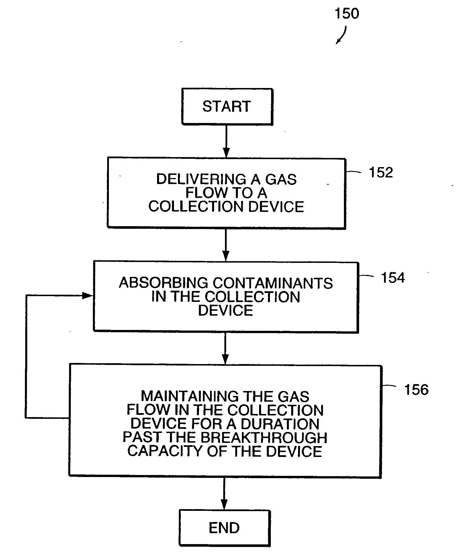
[0053] The present invention is directed to a system and method for determining and controlling contamination. Preferred embodiments of the present invention address gaseous contamination as well as the contaminants adsorbed on surfaces, for example, an optical surface. The latter is more critical to the performance of the optical elements.

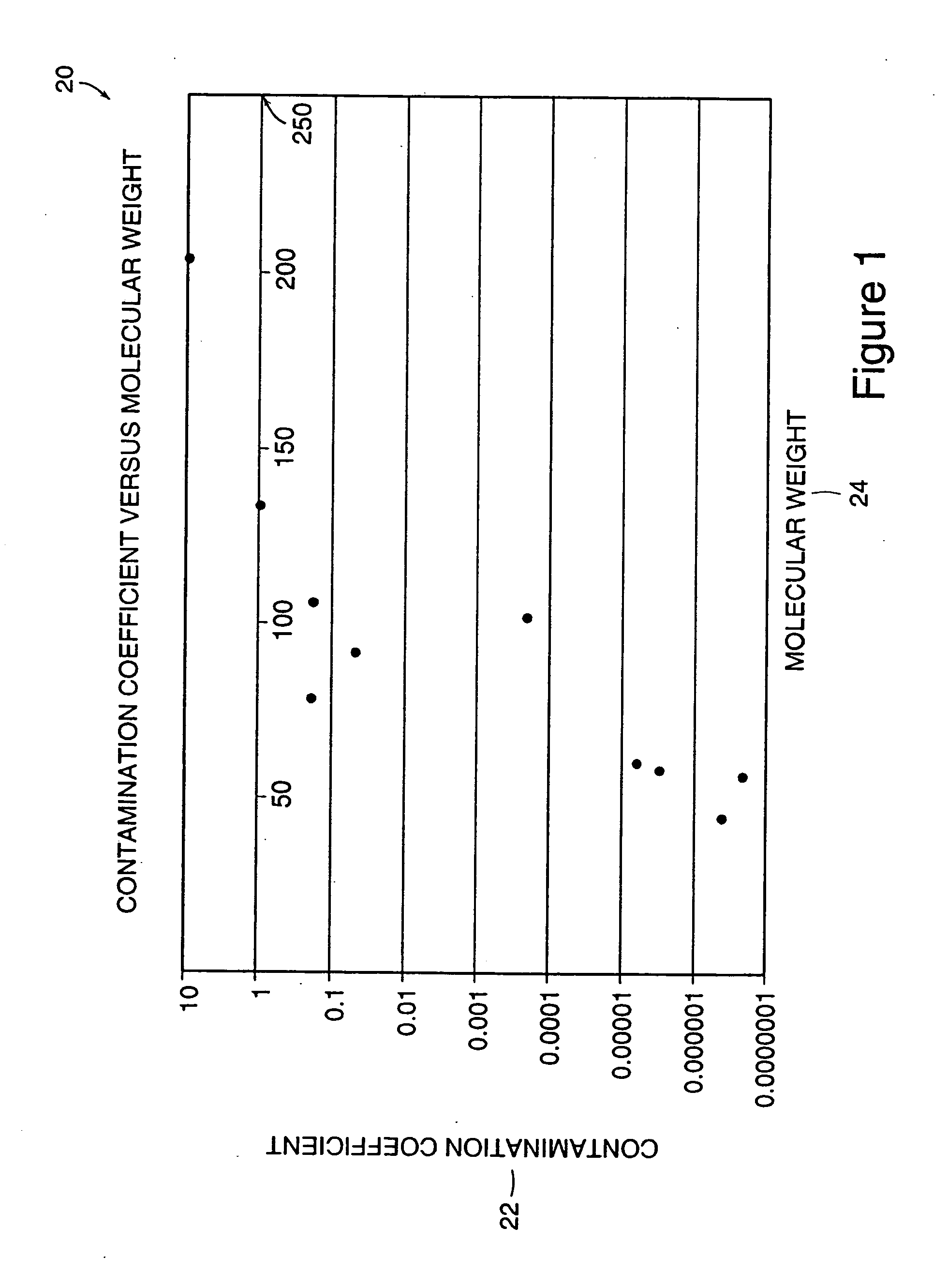
[0054] Table 1 illustrates various species in a cleanroom environment, such as, for example, a fabrication environment using photolithography systems. The low molecular weight species, such as acetone, isopropyl alcohol and low molecular weight siloxanes are the most prevalent in manufacturing environments. Compounds that are most likely to reduce the performance of optics are compounds having a high contamination coefficient or a high molecular weight examples can include, but are not limited to, methoxytrimethyl silane, trimethyl silane and trimethyl silanol. These compounds appear in italics in Table 1 have a higher molecular weight, higher co...


PUM

PropertyMeasurementUnit
volumesaaaaaaaaaa
volumesaaaaaaaaaa
wavelengthaaaaaaaaaa

Abstract

The present invention provides passive sampling systems and methods for monitoring contaminants in a semiconductor processing system. In one embodiment, that passive sampling system comprises a collection device in fluid communication with a sample line that provides a flow of gas from a semiconductor processing system. The collection device is configured to sample by diffusion one or more contaminants in the flow of gas.

Description

CROSS REFERENCE TO RELATED APPLICATIONS [0001] The present application is a divisional application of U.S. patent application Ser. No. 10 / 662,892 filed Sep. 15, 2003, which is a continuation-in-part of U.S. patent application Ser. No. 10 / 395,834 filed Mar. 24, 2003, which is continuation-in-part of U.S. patent application Ser. No. 10 / 253,401 filed Sep. 24, 2002, now U.S. Pat. No. 6,759,254, which is a continuation-in-part of U.S. patent application Ser. No. 09 / 961,802, filed Sep. 24, 2001, now U.S. Pat. No. 6,620,630. The entire contents of the above patents and applications are incorporated herein by reference.BACKGROUND OF THE INVENTION [0002] Semiconductor manufacturers continue to measure and control the level of contamination in the processing environment, especially during the critical steps of the photolithography processes. The typical means of determining the quality and quantity of contamination in gas samples in cleanroom manufacturing environments involves sampling air a...

Claims


Application Information

Patent Timeline
Patent Type & Authority Applications(United States)
IPC IPC(8): H01L21/00G01N1/00H01L21/66B01D53/22G01N1/22G01N1/40
CPCB01D53/22G01N1/2205H01L21/67253G01N1/405G01N1/2247
Inventor KISHKOVICH, OLEG P.GRAYFER, ANATOLYGOODWIN, WILLIAM M.KINKEAD, DEVON
Owner KISHKOVICH OLEG P
Why Eureka
Try Eureka