Field emission device

a field emission and emission device technology, applied in the manufacture of electrode systems, electric discharge tubes/lamps, discharge tubes luminescnet screens, etc., can solve the problems of complex process techniques, high cost, and inability to achieve the field emission enhancement of a single cn

Inactive Publication Date: 2008-01-17
TSINGHUA UNIV +1
View PDF18 Cites 16 Cited by
  • Summary
  • Abstract
  • Description
  • Claims
  • Application Information

AI Technical Summary

Benefits of technology

[0007]Theoretically, the CNT has small diameter and big slenderness (i.e. diameter / length) ratio thus making the CNT quite a powerful field emission enhancer. However, in practice, like a flat panel display, the field emission enhancer of the entire field emission film cannot achieve the field emission enhancement of a single CNT. As a result, emission voltage of the whole system is increased, and current density is decreased. Meanwhile, the process technique became complicated, and the cost becomes relatively high.

Problems solved by technology

However, in practice, like a flat panel display, the field emission enhancer of the entire field emission film cannot achieve the field emission enhancement of a single CNT.
Meanwhile, the process technique became complicated, and the cost becomes relatively high.

Method used


Image

  • Field emission device
  • Field emission device

Examples


Embodiment Construction

[0012]Reference will now be made to the drawings to describe in detail the preferred embodiment of the field emission device.

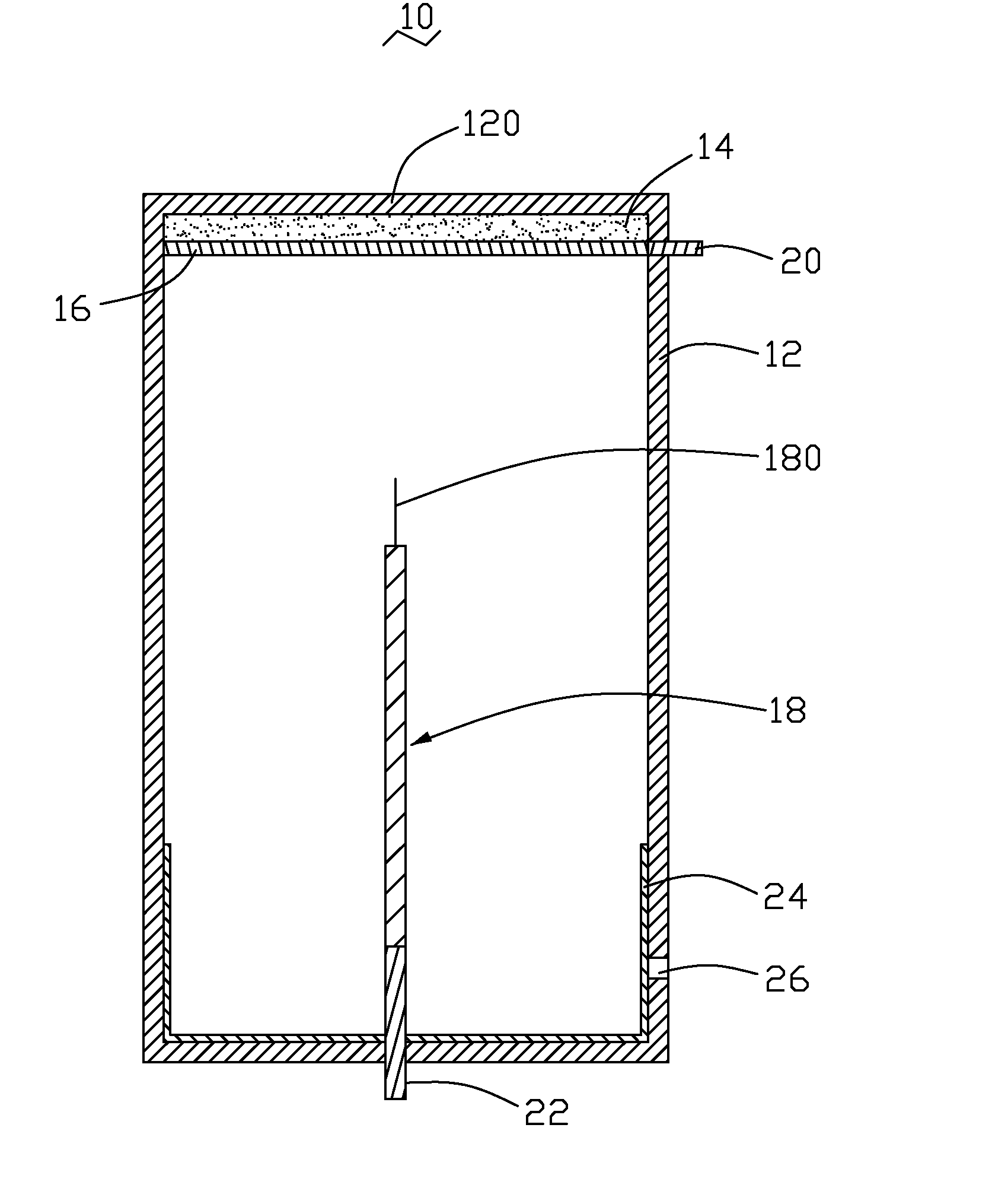
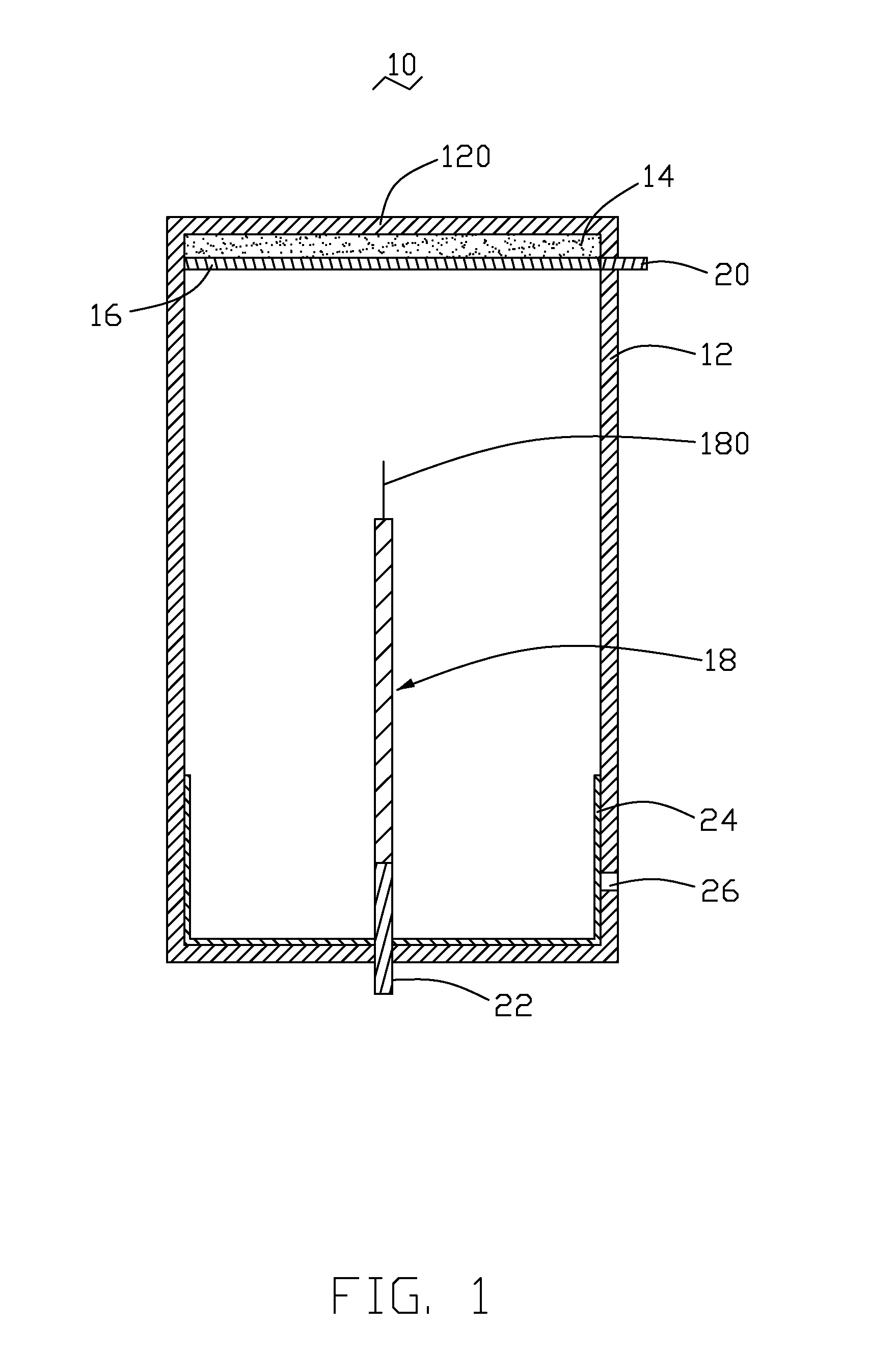
[0013]Referring to FIG. 1, a field emission device 10 includes an light permeable anode 16, a cathode 18 and a sealed container 12 enclosing the light permeable anode 16 and the cathode 18. The sealed container 12 includes a light permeable portion 120 being coated with two overlapping layers inside. A first layer is a phosphor layer 14, and a second layer is a conductive material constituting the light permeable anode 16. In other words, the phosphor layer 14 is sandwiched between the light permeable portion 120 and the light permeable anode 16. The cathode 18 is incorporated in the sealed container 12 facing the light permeable portion 120. A carbon nanotube yarn 180 is attached to the cathode 18 and faces the light permeable portion 120. The light permeable anode 16 as well as the cathode 18 is electrically connected with respective terminals for enabling a...


PUM


Abstract

A field emission device (10) includes a sealed container (12) with a light permeable portion (120). A phosphor layer (14) and a light permeable anode (16) are coated on inside surface of the light permeable portion in succession. A cathode (18) is enclosed in the sealed container. A carbon nanotube yarn is attached to the cathode facing the light permeable portion. Before being embedded into the sealed container, the carbon nanotube yarn is processed in the following steps: providing a carbon nanotube array, drawing out at least one carbon nanotube yarn string from the carbon nanotube array, treating the at least one carbon nanotube yarn string using an organic solvent in a manner such that the at least one carbon nanotube yarn string is formed into a single strand of carbon nanotube yarn, and heating the single strand of the carbon nanotube yarn.

Description

CROSS REFERENCE TO RELATED APPLICATION[0001]This application is related to commonly-assigned copending application Ser. No. ______, entitled “METHOD FOR MAKING CARBON NANOTUBE-BASED DEVICE” (attorney docket number US 9507), and Ser. No. ______, entitled “CARBON NANOTUBE YARN AND METHOD FOR MAKING THE SAME” (attorney docket number US 9508). Disclosures of the above-identified application are incorporated herein by reference.BACKGROUND OF THE INVENTION[0002]1. Field of the Invention[0003]The present invention relates to field emission devices, and more particularly to a field emission device.[0004]2. Description of Related Art[0005]Field emission devices are based on emission of electrons in a vacuum. Electrons are emitted from micron-sized tips in a strong electric field, and the electrons are accelerated and collide with a fluorescent material. The fluorescent material then emits visible light. Field emission devices are thin, light weight, and provide high levels of brightness.[000...

Claims


Application Information

Patent Timeline
Patent Type & Authority Applications(United States)
IPC IPC(8): H01J1/00H01J19/06
CPCB82Y10/00H01J9/025H01J2329/86H01J2201/30469H01J31/123
Inventor YANG, YUAN-CHAOWEI, YANGLIU, LIANGJIANG, KAI-LIFAN, SHOU-SHAN
Owner TSINGHUA UNIV
Why Eureka
Try Eureka