Selective metal patterns using polyelect rolyte multilayer coatings

a multi-layer coating and selective metal technology, applied in the direction of coatings, printed circuit manufacturing, liquid/solution decomposition chemical coatings, etc., can solve the problems of limiting the functionality of substrates and other materials, expensive device fabrication steps, and inability to function properly, so as to achieve stable coating, reduce fabrication costs, and increase economic

Inactive Publication Date: 2008-01-17
BOARD OF TRUSTEES OPERATING MICHIGAN STATE UNIV
View PDF3 Cites 17 Cited by
  • Summary
  • Abstract
  • Description
  • Claims
  • Application Information

AI Technical Summary

Benefits of technology

[0011] The drawbacks and limitations of the known technology have been overcome with the discovery and development of the present processes for creating versatile and selective metal patterns (such as copper and nickel) by combining PEM coatings, microcontact printing (MCP), and electroless deposition (ELD). MCP is used to pattern a charged catalyst (such as palladium, stannous ions, and the like) onto oppositely charged PEM coated substrates. PEMs, unlike silanes and thiols, can be stably coated onto virtually any substrate including hydrophobic polymer surfaces. This results in a highly selective, electrostatically bound charged catalyst ion complex on the PEM coated substrates. The substrate is then placed into an ELD bath where a metal, such as nickel or copper selectively plates only at the catalyzed regions. In various embodiments, the system, which involves PEMs as the stable adhesion layer, is more versatile, more economical, and works over a larger range of substrates than previous approaches. The combination of PEMs and MCP allows the control of 3D features on the micron and submicron scale. Stable and selective metal patterns can be created with nanometer dimensions on flexible substrates, which can result in lower fabrication costs to produce flexible display electronic circuits, sensors, RFID transponders, and other nano- or microelectronic devices.

Problems solved by technology

Most of these techniques are surface-specific; when the substrates are changed these techniques fail to function properly.
However, this process is an expensive step in device fabrication, limits the functionality of substrates and other materials, and has an inability to work with curved substrates or the complex 3D structures needed for new electronic devices.
By using MCP and ELD, numerous devices can be fabricated from a single photolithographic step; however devices produced solely from photolithography require the expensive photolithographic step to be repeated once per device.
While these adhesion layers are effective, they are limited because they form substrate specific bonds that are not interchangeable like electrostatic charges.
This approach is limited by the ink-jet printing resolution which is at best 20 μm.
In addition, the directed self-assembly of charged catalysts onto functionally patterned surfaces often leads to poor selectivity of metal patterns on surfaces.

Method used


Image

  • Selective metal patterns using polyelect rolyte multilayer coatings
  • Selective metal patterns using polyelect rolyte multilayer coatings
  • Selective metal patterns using polyelect rolyte multilayer coatings

Examples


Embodiment Construction

Experimental Details

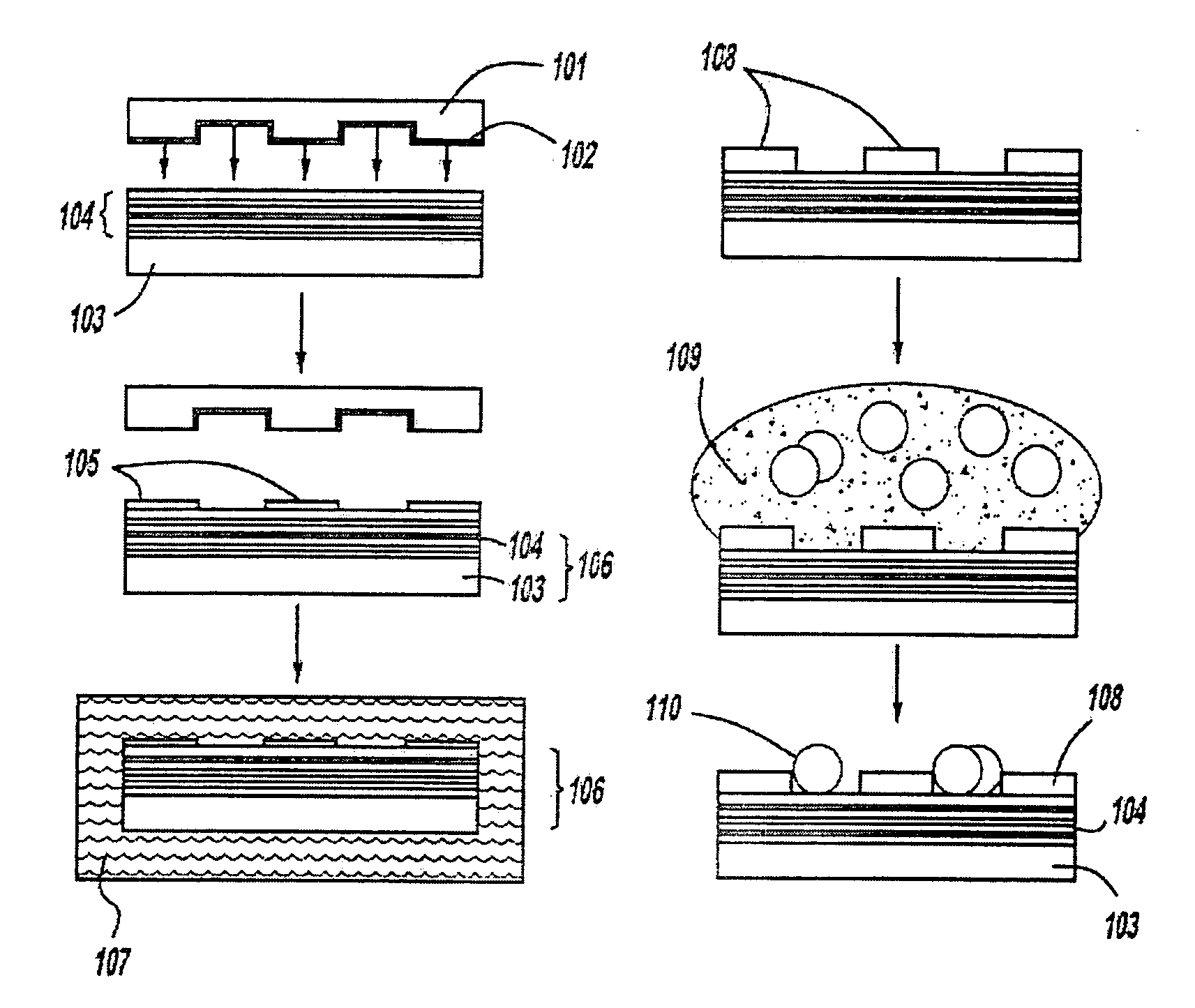
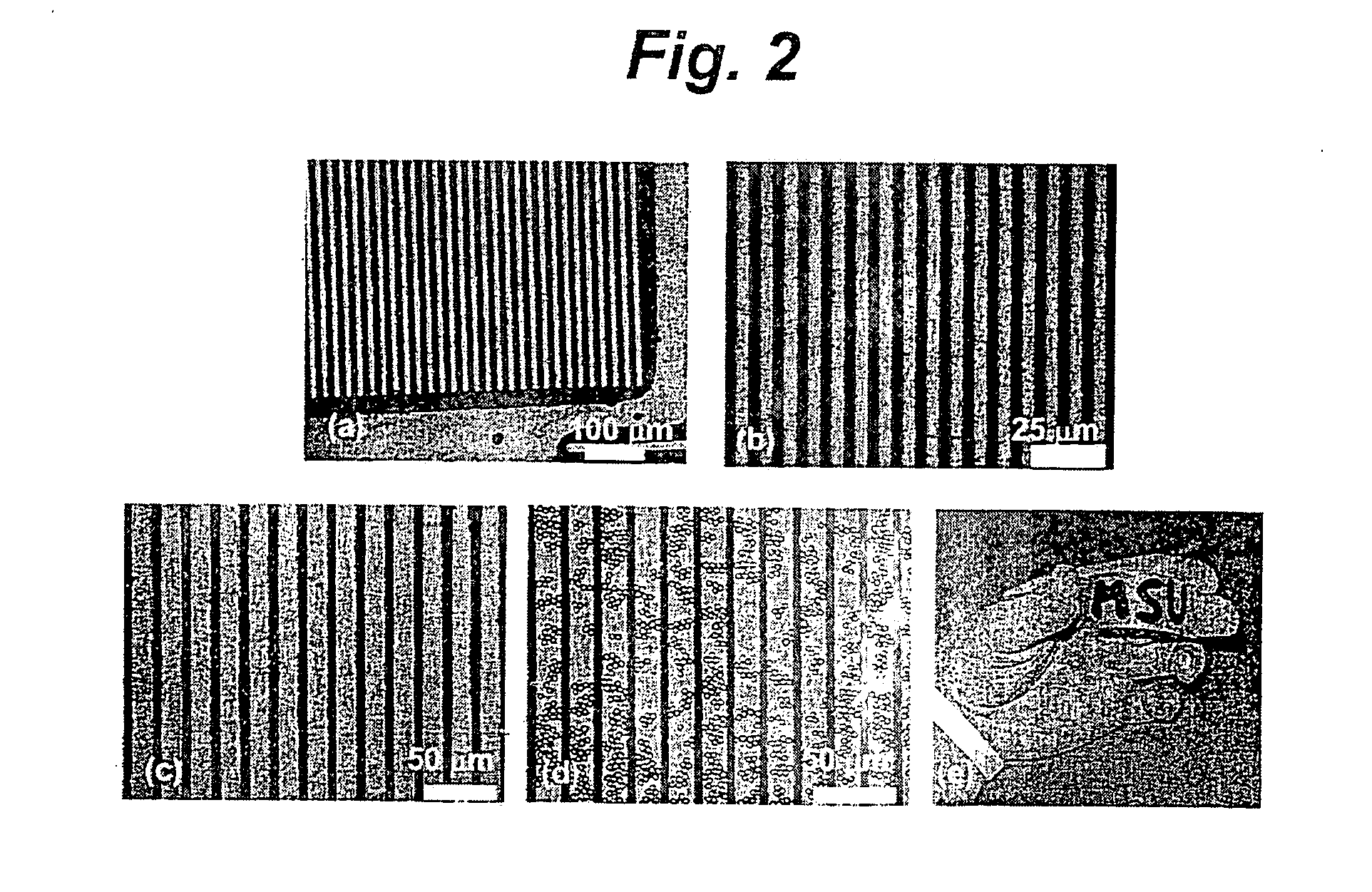
Substrate Preparation—Coating of Substrates with PEM

[0041] To demonstrate the versatile and selective metal patterning process on virtually any surface type, hydrophilic glass and hydrophobic polystyrene substrates were selected. Glass microscope slides (Corning Glass Works, Corning, N.Y.) were sonicated with a Branson ultrasonic cleaner (Branson Ultrasonics Corporation, Danbury, Conn.) for 20 minutes in an Alconox (Alconox Inc., New York, N.Y.) solution followed by 10 minutes of sonication in water. The slides were then blown dry with nitrogen and plasma cleaned (Harrick Scientific Corporation, Broadway Ossining, N.Y.) with oxygen at ˜13.3 Pa for 10 minutes. Before use, polystyrene microscope slides (Nalge Nunc International, Rochester N.Y.) and flexible polyester transparency films (3M, St. Paul, Minn.) were plasma treated under the same conditions for 10 minutes. A Carl Zeiss slide stainer equipped with a custom-designed ultra sonication bath (Advanced Son...


PUM

PropertyMeasurementUnit
inter-feature distancesaaaaaaaaaa
thicknessaaaaaaaaaa
contact timeaaaaaaaaaa

Abstract

Processes for creating versatile and selective metal patterns (such as copper and nickel) combine the use of PEM coatings, microcontact printing (MCP), and electroless deposition. MCP is used to pattern a charged catalyst (such as palladium and stannous ions) onto oppositely charged PEM coated substrates. The substrate is then placed into an electroless deposition bath where a metal selectively plates at the catalyzed regions.

Description

CROSS-REFERENCE TO RELATED APPLICATIONS [0001] This application claims the benefit of U.S. Provisional Application No. 60 / 814,705, filed on Jun. 16, 2006. The disclosure of the above application is incorporated herein by reference.INTRODUCTION [0002] The present disclosure relates to selective metal patterns applied to flexible substrates using polyelectrolyte multilayer (PEM) coatings. [0003] Inexpensive metal patterning techniques with high selectivity have been the focus of current research in displays, radio frequency identification (RFID) transponders, sensors and other nano- and microelectronic device fabrication. Recently, many techniques have been developed to pattern metals on surfaces. Most of these techniques are surface-specific; when the substrates are changed these techniques fail to function properly. A more general and versatile approach to patterning metals is demanded for current and rapidly changing microelectronic applications. [0004] Photolithography based top-d...

Claims


Application Information

Patent Timeline
Patent Type & Authority Applications(United States)
IPC IPC(8): B05D3/10
CPCB82Y30/00C23C18/1608C23C18/2086C23C18/31H05K2203/0709C23C18/40H05K3/182H05K2203/0108C23C18/32
Inventor LEE, ILSOONHENDRICKS, TROY
Owner BOARD OF TRUSTEES OPERATING MICHIGAN STATE UNIV
Why Eureka
Try Eureka