
Semiconductor light-emitting diode

a semiconductor and light-emitting diode technology, applied in the direction of semiconductor devices, basic electric elements, electrical appliances, etc., can solve the problems of lowering the light-emitting efficiency, difficulty in uniform current supply, and low current quantity, and achieve the effect of high light-emitting efficiency and increasing the efficiency of light extraction

Inactive Publication Date: 2008-01-24
MITSUBISHI ELECTRIC CORP
View PDF6 Cites 25 Cited by
  • Summary
  • Abstract
  • Description
  • Claims
  • Application Information

AI Technical Summary

Benefits of technology

[0014]To solve the problems as described above, it is an object of the present invention to provide a semiconductor light-emitting diode that can achieve a high light emitting efficiency by uniformly supplying a current to a light emitting layer and by raising the efficiency of light extracting.
[0016]According to the present invention, a high light emitting efficiency can be achieved by uniformly supplying a current to a light emitting layer and by raising the efficiency of light extracting.

Problems solved by technology

However, since there is a large lattice mismatch between the sapphire substrate and the crystals of a nitride semiconductor grown on the substrate, when the nitride semiconductor is directly grown on the sapphire substrate, a very large number of threading dislocations having a density of 109 to 1010 cm−3 or higher are present in the light-emitting layer.
However, when the opening width L of the electrodes 7 was reduced, as Fig.7 shows, there was a problem wherein a part of the light generated from the light-emitting layer was reflected or absorbed by the p-electrode 7 causing the lowering of the light emitting efficiency.
However, even in this case, the light is reflected and absorbed, and when the light emitting wavelength of a semiconductor light-emitting diode is short, a serious problem arises.
Also when the electrode is thin, since the resistance of the electrode elevates, the quantity of current lowers to the location far from the wire for current supply, and the uniform current supply is difficult.
However, since the n-electrode 6 becomes apart from the p-electrode 7, it is difficult to uniformly supplying the current.
Furthermore, since the distance between the n-electrode 6 and the p-electrode 7 is shortened, there is a problem wherein it is difficult to die-bond with both electrodes insulated.

Method used


Image

  • Semiconductor light-emitting diode
  • Semiconductor light-emitting diode
  • Semiconductor light-emitting diode

Examples


first embodiment

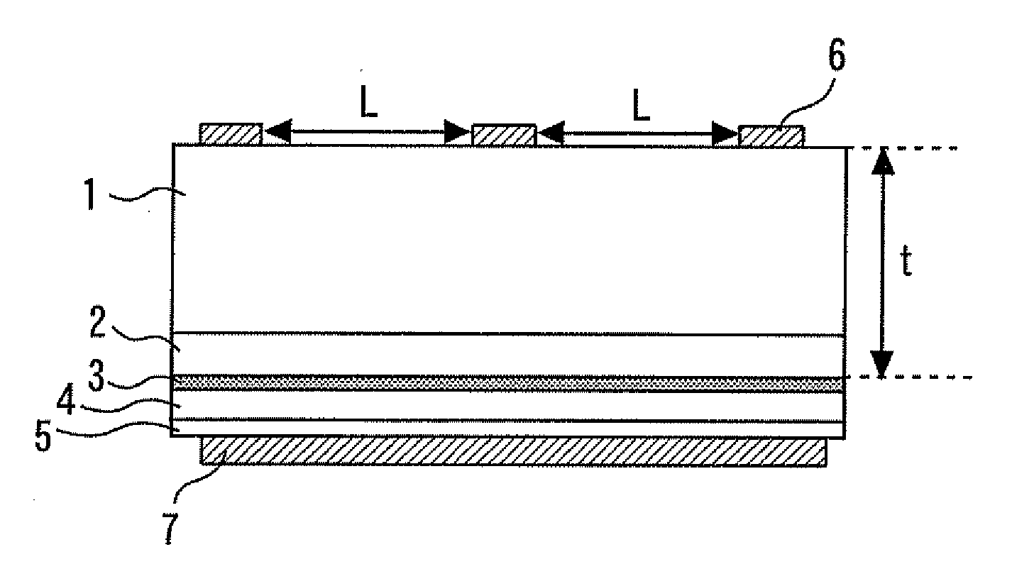
[0023]FIG. 1 is a sectional view showing a semiconductor light-emitting diode according to a first embodiment of the present invention. A GaN substrate 1 is a conductive substrate light transmissive to light-emitting wavelengths, and the thickness thereof is made to be 99 μm by polishing. On the GaN substrate 1, as semiconductor layers, an n-type AlGaN clad layer 2 having a thickness of 1.0 μm and an Al composition ratio of 0.07; a light-emitting layer 3 composed of four InGaN barrier layers each having a thickness of 7 nm and an In composition ratio of 0.02 not shown and three InGaN well layers each having a thickness of 5 nm and an In composition ratio of 0.10; a p-type AlGaN clad layer 4 having a thickness of 100 nm and an Al composition ratio of 0.07; and a p-type GaN contact layer Shaving a thickness of 20 nm are laminated.

[0024]A p-electrode 7 (principal-surface electrode) composed of Pd / Au is formed on the substantially entire surface of the GaN contact layer 5, and an n-elec...

second embodiment

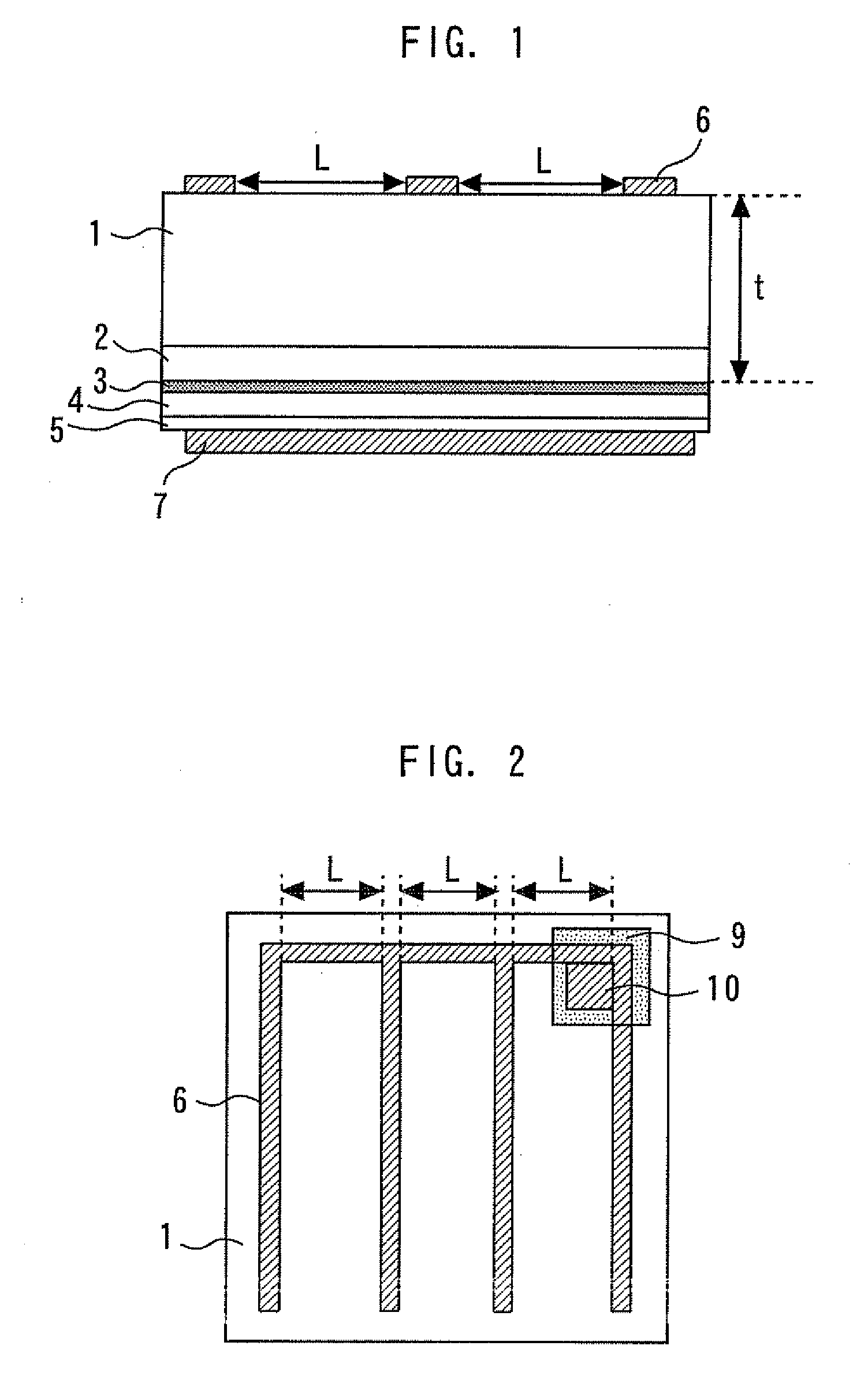
[0035]FIG. 4 is a diagram of a semiconductor light-emitting diode according to the second embodiment of the present invention when viewing from the back face. The size of the element is 400 μm×400 μm. The n-electrode 6 is comb-shaped, the width of the n-electrode 6 is 15 μm, and the width L of an opening is 150 μm. The size of the electrode pad 10 is 50 μm×50 μm, and the size of the SiO2 insulating film 9 is 60 μm×60 μm. Since the laminate structure of the element is the same as in the first embodiment, the description thereof will be omitted.

[0036]In the second embodiment, L=1.5 t, and the proportion of the area of the n-electrode 6 to the area of the rear surf ace of the substrate 1 is about 13%. As a result, the light emitting wavelength at 20 mA is 408 mm, and the external quantum efficiency is 38%, which means that a very high light emitting efficiency can be obtained.

third embodiment

[0037]FIG. 5 is a diagram of a semiconductor light-emitting diode according to the third embodiment of the present invention when viewing from the back face. The size of the element is 400 μm×400 μm. The n-electrode 6 is net-shaped, the width of the n-electrode 6 is 20 μm, and the width L of an opening is 100 μm. The size of the electrode pad 10 is 50 μm×50 μm, and the size of the SiO2 insulating film 9 is 60 μm×60 μm. Since the laminate structure of the element is the same as in the first embodiment, the description thereof will be omitted.

[0038]In the third embodiment, L=1.0 t, and the proportion of the area of the n-electrode 6 to the area of the rear surface of the substrate 1 is about 34%. As a result, the light emitting wavelength at 20 mA is 408 mm, and the external quantum efficiency is 31%, which means that a very high light emitting efficiency can be obtained.

[0039]In the above-described first to third embodiments, the cases wherein the n-electrodes 6 were a comb shaped or...


PUM


Abstract

A semiconductor light-emitting diode includes an electrically conductive substrate transmissive to light-emitting wavelengths, and semiconductor layers including a light-emitting layer, on the substrate. A principal-surface electrode is located on the semiconductor layers and a rear-surface electrode having an opening is located on the rear surface of the substrate. The width of the opening is L, the distance between the rear-surface electrode and the light-emitting layer is t, L≦2 t, and the rear-surface electrode covers no more than 40% of the rear surface of the substrata.

Description

BACKGROUND OF THE INVENTION [0001]1. Field of the Invention[0002]The present invention relates to a nitride semiconductor light-emitting diode fabricated on a light transmissive and conductive substrate, such as a GaN substrate, and more specifically to a semiconductor light-emitting diode that can achieve a high light-emitting efficiency by uniformly supplying a current to a light-emitting layer and raising the light extraction efficiency.[0003]2. Background Art[0004]In recent years, the research and development of blue, white or ultraviolet semiconductor light-emitting diodes (LEDs) using a nitride-containing III-V group compound semiconductor, such as AlInGaN, have been carried out, and already in practical use (for example, refer to Japanese Patent Laid-Open No. 2005-166840). The mainstream of present semiconductor light-emitting diodes is of a type wherein the crystals of a nitride semiconductor are grown on a sapphire substrate because of the low costs thereof.[0005]However, s...

Claims


Application Information

Patent Timeline
IPC IPC(8): H01L33/00H01L33/32H01L33/38H01L33/40H01L33/44
CPCH01L33/38
Inventor KURAMOTO, KYOSUKE
Owner MITSUBISHI ELECTRIC CORP
Learn More