Imaging thin film structures by scanning acoustic microscopy

a thin film structure and scanning acoustic microscopy technology, applied in the direction of instruments, specific gravity measurement, measurement devices, etc., can solve the problems of increasing the difficulty in non-destructively differentiating features of multi-layer structures, poor z-direction resolution of x-ray imaging, and increasing the demand for enhanced spatial resolution

Inactive Publication Date: 2008-01-31
IBM CORP
View PDF16 Cites 20 Cited by
  • Summary
  • Abstract
  • Description
  • Claims
  • Application Information

AI Technical Summary

Benefits of technology

[0027]In accordance with this invention, apparatus for Scanning Acoustic Microscopy (SAM) of a semiconductor device, with the semiconductor device having a first surface and a second surface with bonding features secured to the first surface us provided. It comprises a container for retaining acoustic transmission fluid in contact with the second surface with the bonding features. A chamber surrounds the first surface. The chamber has an interior space filled with an atmosphere selected from a gas and a vacuum and being sealed to prevent the acoustic transmission fluid from being admitted into the interior space. An acoustic scanning probe of a SAM is positioned confronting the second surface of the semiconductor device.
[0028]Preferably, the bonding features comprise Ball-Limiting Metallurgy (BLM) pads and solder bonding elements. Preferably, the bonding features comprise Ball-Limiting Metallurgy (BLM) pads, solder bonding elements and a substrate. Preferably, the container includes a sealed chamber secured to the first surface of the semiconductor device with forming a gas chamber separating the bonding features from the acoustic transmission fluid. Preferably, the acoustic transmission fluid comprises water, and the container includes a sealed chamber secured to the first surface of the semiconductor device with the sealed chamber comprising a gas filled chamber separating the bonding features from the water.
[0029]Preferably, the acoustic transmission fluid comprises water, and the container includes a sealed vacuum chamber secured to the first surface of the semiconductor device with the sealed vacuum chamber separating the bonding features from the water. Preferably, the acoustic transmission fluid comprises water, and the container includes an impervious, physical barrier secured to the first surface of the semiconductor device separating the bonding features from the water.
[0030]In accordance with another aspect of the invention, apparatus for Scanning Acoustic Microscopy (SAM) of a semiconductor device having a first surface and a second surface with bonding features secured to the first surface comprises a tank for retaining acoustic transmission fluid. An impervious fixture is retained in sealed contact with the first surface defining an interior space surrounding the bonding features, the impervious fixture being filled with an atmosphere of gas and being sealed to exclude the acoustic transmission fluid from admission to the interior space.
[0031]In accordance with still another aspect of this invention a method of testing a semiconductor device employs Scanning Acoustic Microscopy (SAM) of a semiconductor device having a first surface and a second surface with bonding features secured to the first surface. The steps involve retaining acoustic transmission fluid in a container in contact with the second surface; providing a chamber surrounding the first surface, the chamber having an interior space filled with an atmosphere selected from an atmosphere of gas and a vacuum with the chamber being sealed to prevent the acoustic transmission fluid from being admitted into the interior space; and positioning a SAM acoustic scanning probe confronting the second surface of the semiconductor device extending into the acoustic transmission fluid.
[0032]Preferably, the container includes a sealed chamber secured to the first surface of the semiconductor device forming a gas chamber separating the bonding features from the acoustic transmission fluid.

Problems solved by technology

As chip sizes becomes progressively smaller and as the interconnect density therein increases, the demand for enhanced spatial resolution becomes greater and the difficulty in non-destructively differentiating features in the multi-layer structure increases.
Typically, the Z-direction resolution for x-ray imaging is quite poor.
For example, an acoustic microscope can detect an air void as thin as 500 Å between a bond and a silicon wafer, but it is difficult to differentiate features in a multilayer metal stack with a thickness of a few thousands angstroms.
In selective etching, the etching chemistries employed can create a serious problem by attacking a BLM pad or UBM structure preferentially thereby reducing the diameter of the UBM and diminishing the mechanical integrity of the C4 bumps attached to the BLM pads.
That is a serious concern because it reduces the degree of reliability of the bonds formed between the elements being processed.
Problems referred to as undercutting or over-etching can be caused by fluid flow characteristics in the bath, location in a wafer boat, and etch chemistries.
Thus problems caused by over-etching or undercutting effects are concerns with regard to the reliability of C4 interconnects.
Those problems are exacerbated as the density of interconnect structures increases and as the scale of the BLM pads and C4 bumps becomes smaller and smaller.
Both methods are destructive and time consuming.
As stated above, there is a significant problem with immersion in the water 22 of a device under test for inspection by a C-SAM testing apparatus.
The problem is that water is an excessively good transmitter of acoustic waves.
The edge effect attributable to the scattering of the acoustic waves introduces additional error in measurement.
The small difference in acoustic impedance in the material reduces contrast.
In summary, it has been found that there is a significant problem with immersing a sample to be inspected by a C-SAM testing apparatus in water 22.
The problem is that water 22 is a good transmitter of acoustic waves.

Method used


Image

  • Imaging thin film structures by scanning acoustic microscopy
  • Imaging thin film structures by scanning acoustic microscopy
  • Imaging thin film structures by scanning acoustic microscopy

Examples


first embodiment

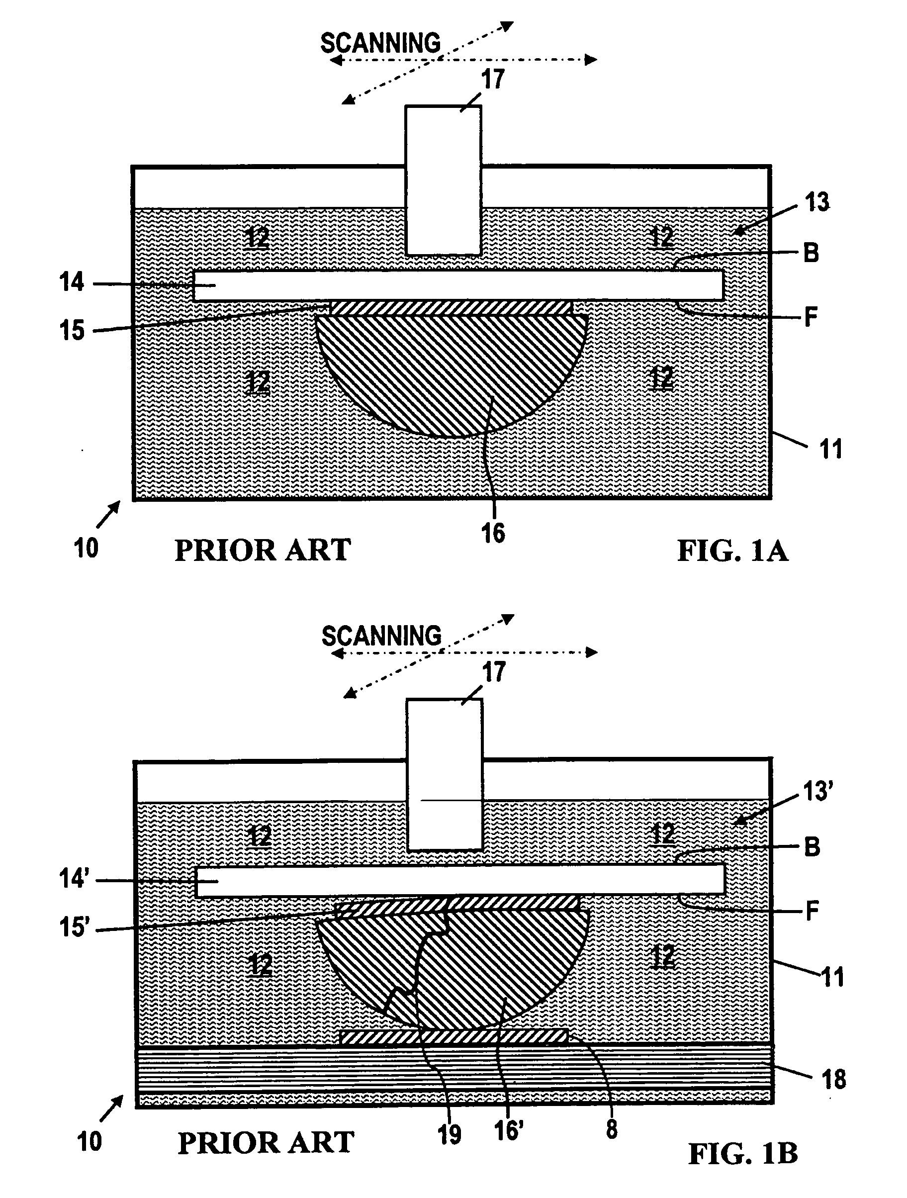
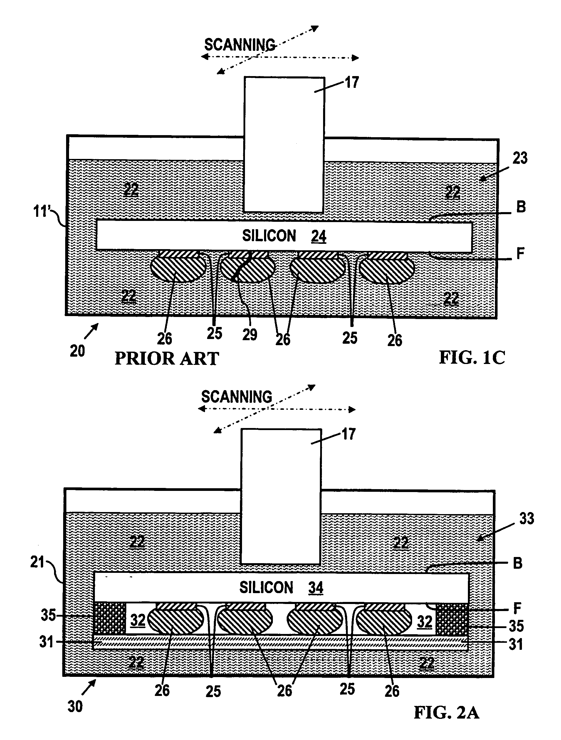
[0052]FIG. 2A is an illustration of sample setup in accordance with the present invention wherein C-SAM acoustic microscopy is performed by immersion of a Device Under Test (DUT) 33 in water 22 to couple of acoustic energy to the back surface B of the device 33 while isolating the front portion F of the device 33 including multiple C4 solder bumps 26 bonded to multiple BLM pads 25 in a, sealed, dry 32 protected from the water 22 in which the device 33 is immersed with a solid plate 31 and a gasket 35 sealed to the C4 solder bump (front) side F of the device 33 to maintain the BLM pads and C4 solder bumps enveloped in environment of air in chamber 32.

[0053]In particular, in FIG. 2A an acoustic microscope is employed in a configuration in accordance with this invention comprising a C-SAM testing arrangement 30 including a tank 21 filled with water 22. The testing apparatus shown in FIG. 2A is provided for testing a device 33 which includes a silicon wafer 34. The device 33 is immersed...

second embodiment

[0057]FIG. 2B is an illustration of a modification of the sample setup in FIG. 2A in accordance with the present invention, wherein multiple BLM pads 25 and multiple C4 solder bumps 26 are isolated in a dry environment within a sealed enclosure 42. In other words, the C4 solder bumps 26 and BLM pads 25 are isolated from the water 22. The sealed enclosure 42 is evacuated through a vacuum line 47 connected to the sealed enclosure 42. In FIG. 2B the seal to the front surface F of the silicon, semiconductor wafer 44 is retained in place by a vacuum chuck so the solder bumps 26 and BLM pads 25 remain in vacuum, isolated from water 22, during scanning. Sound waves are substantially blocked from being transmitted by the very high impedance of a partial vacuum, and are substantially completely reflected back to the interface.

[0058]The provision of a vacuum within the enclosure 42 is an improvement over the air provided in FIG. 2A, because the higher impedance of the vacuum will transmit alm...

third embodiment

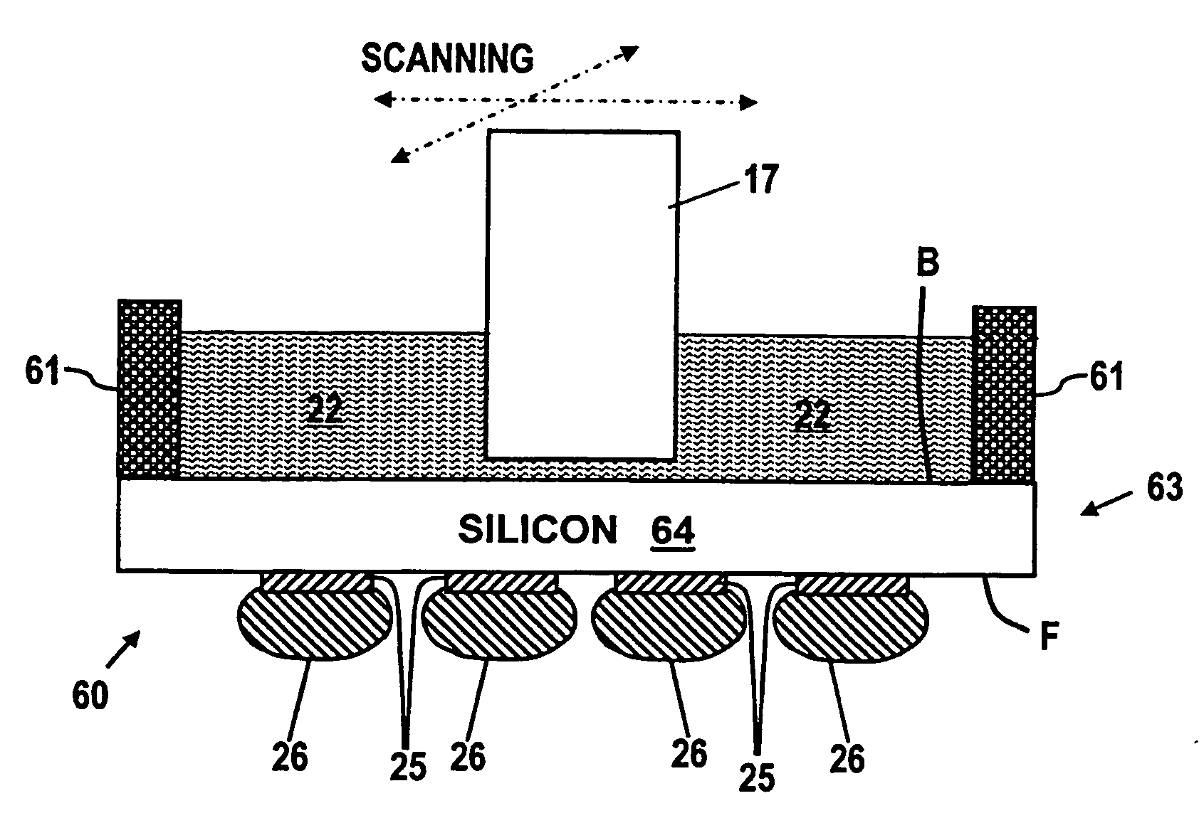
[0062]FIG. 2C is an illustration of sample setup in accordance with the present invention wherein C-SAM acoustic microscopy is performed by partial immersion of a device 63. That is achieved by forming a dam retaining a sufficient depth of water 22 above the back surface B of a device 63 to couple of acoustic energy from the bottom end of the SAM probe 17 to the back surface B of the device 63. The inverted front surface F of the device 63 (including the multiple BLM pads 25 which are bonded to multiple C4 solder bumps 26) is located in a dry, open air environment isolated from the water 22. In summary, in FIG. 2C, the dam 61, and the back B of the substrate 64 included in the device 63 form a container above the substrate 64 wherein water 22 is confined.

[0063]The water 22 is deep enough to covers the bottom end of the transducer 17. The dam 61 comprises an impervious, physical barrier 61 on the periphery of the back surface B of the substrate 64. The physical barrier 61 may compris...


PUM

PropertyMeasurementUnit
frequenciesaaaaaaaaaa
thicknessaaaaaaaaaa
thicknessaaaaaaaaaa

Abstract

A method and apparatus for Scanning Acoustic Microscopy (SAM) for testing of a semiconductor device having a first surface and a second surface with bonding features secured to said first surface are provided. An impervious fixture comprising a dam or a tank retains acoustic transmission fluid in contact with the second surface. Acoustic transmission fluid is excluded from admission to the space surrounding the bonding features where an atmosphere of gas or a vacuum is provided by isolating the first surface from the acoustic transmission fluid either by providing a sealed chamber protecting the first surface or by providing a dam surrounding the second surface.

Description

BACKGROUND OF THE INVENTION[0001]The present invention relates to the non-destructive inspection of the microscopic structures by acoustic microscopy. More particularly, it is related to the use of Scanning Acoustic Microscopy (SAM) to perform non-destructive imaging of the internal structure of a silicon wafer or semiconductor packaging materials.[0002]Non-destructive inspection of the electronics packaging by acoustic microscopy or x-ray imaging has been widely used in semiconductor industry for quality assurance and failure analysis. In particular, Scanning Acoustic Microscopy (SAM) technology has been widely used for non-destructive inspection in the electronics packaging industry. Non-destructive SAM is an analytic technique using ultrasound waves to detect changes in acoustic impedances in integrated circuits (ICs) and other similar materials. In SAM analysis, pulses of acoustic waves at different frequencies are generated which penetrate various materials and the reflections ...

Claims


Application Information

Patent Timeline
Patent Type & Authority Applications(United States)
IPC IPC(8): G01N29/04
CPCG01N29/0681G01N29/225G01N2291/044G01N2291/0231G01N29/28
Inventor LU, MINHUA
Owner IBM CORP
Why Eureka
Try Eureka