Multi-Layer Capacitor and Mold Capacitor

Inactive Publication Date: 2008-02-07
PANASONIC CORP
View PDF13 Cites 20 Cited by
  • Summary
  • Abstract
  • Description
  • Claims
  • Application Information

AI Technical Summary

Benefits of technology

[0017] This invention has been accomplished in order to attain the above problem. An object of this invention is to provide a multilayer capacitor and mold capacitor which can realize a high withstand voltage without hindering downsizing and implementation of high capacitance.

Problems solved by technology

Thus, stress concentration at the center (center in the width direction of the dielectric substrate) of the regions where the internal electrodes are adjacent is most problematic.
This presented a problem that the level in the withstand voltage corresponding to the voltage stress differs between the center to which more stress is concentrated and the end.
As a result, the entire structure of the multilayer capacitor does not have the structure optimized for the withstand voltage.
As a result, the withstand voltage of the multilayer capacitor could not be surely improved.
This was a significant problem in the cases where the downsizing of devices is demanded.

Method used


Image

  • Multi-Layer Capacitor and Mold Capacitor
  • Multi-Layer Capacitor and Mold Capacitor
  • Multi-Layer Capacitor and Mold Capacitor

Examples


embodiment 1

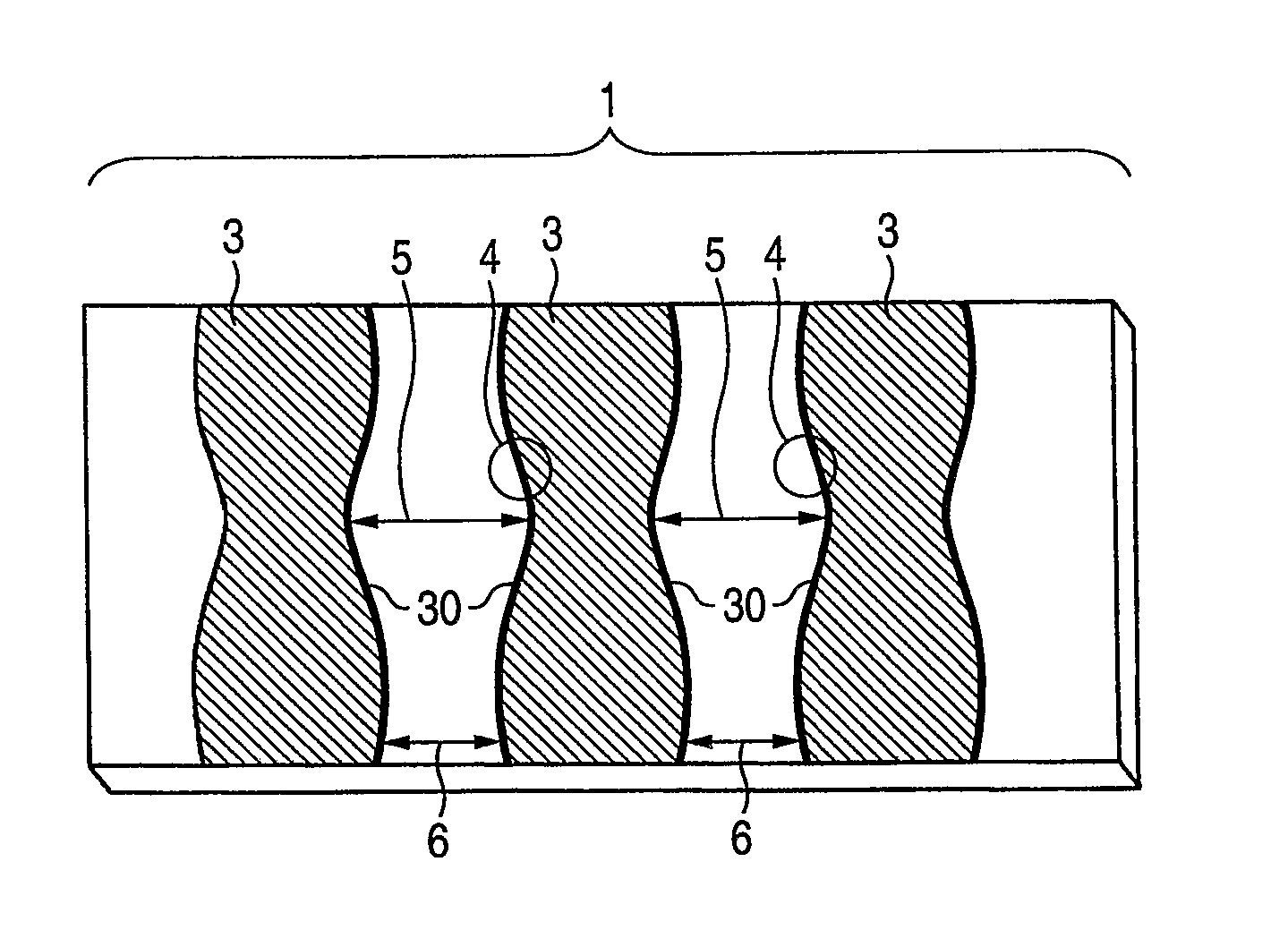
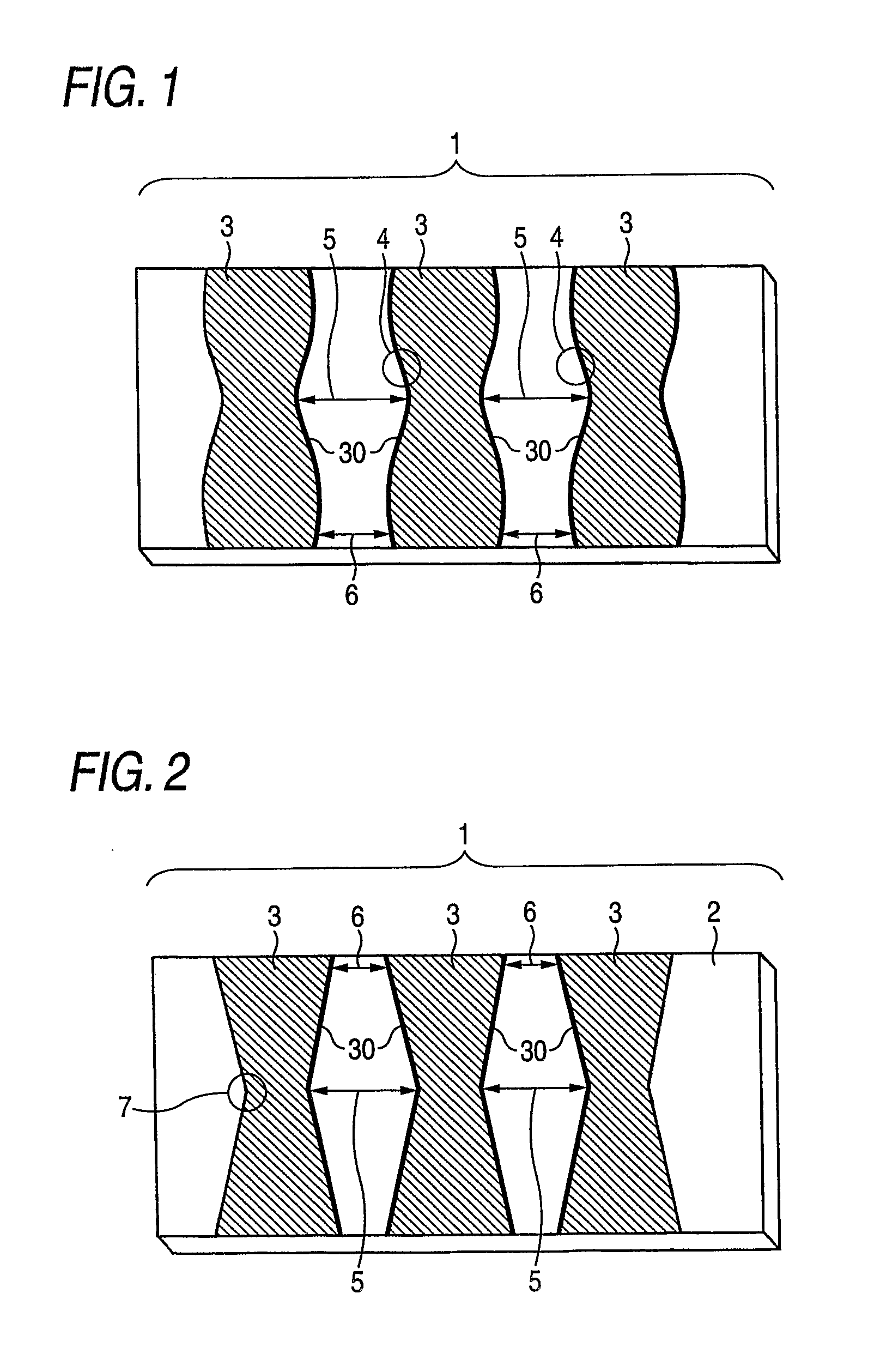
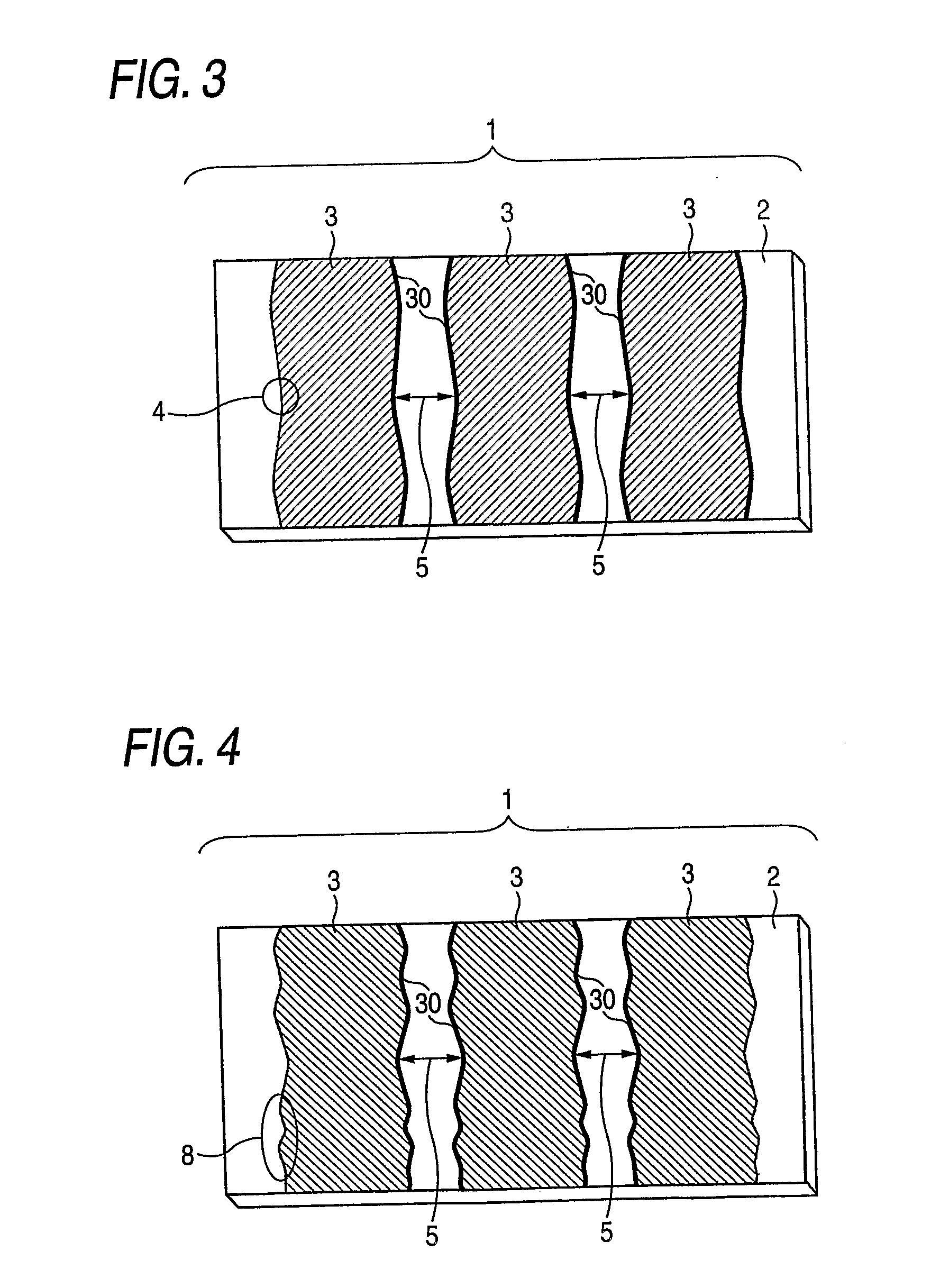
[0027]FIGS. 1, 2, 3, 4, 5 and 6 are a top view of a dielectric substrate for layering according to the first embodiment of this invention, respectively. FIG. 7 is a side sectional view of a multilayer capacitor according to this embodiment. FIG. 8 is a side sectional view of a mold capacitor according to this embodiment. FIG. 9 is an entire perspective view of the mold capacitor according to this embodiment. FIG. 10 is a graph showing the relationship between the serge breakdown voltage and capacitance in the multilayer capacitor according to this invention.

[0028] In these figures, reference numeral 1 denotes a layered dielectric substrate; 2 a dielectric substrate; 3 an internal electrode; 4 a constriction; 5 a maximum interval zone; 6 a minimum interval zone; 7 a dent; 8 a wavy area; 9 a terminal electrode; 10 a mulitilayer capacitor; 11 a package; 12 a lead terminal; and 20 a mold capacitor.

[0029] First, a detailed explanation will be given of each component.

[0030] First, the ...

embodiment 2

[0078] FIGS. 11 to 19 are a side view of the multilayer capacitor according to the second embodiment of this invention, respectively.

[0079] In these figures, reference numeral 11 denotes a multilayer capacitor; 12 a substrate; 13 a terminal electrode; 14 denotes a lead wire; 15 a contact region; 16 a filling space; 17 an internal electrode; and 18 a package.

[0080] First, a detailed explanation will be given of each component.

[0081] First, the substrate 12 will be explained.

[0082] The substrate 12 is a substrate of a dielectric material, which is preferably e.g. titanium oxide or barium titanate. The dielectric material may be alumina. According to the desired dielectric constant (the value of capacitance can be adjusted by the dielectric constant) and material strength of these oxide-series dielectric material, metallic dielectric material and ceramic-series dielectric material, the material and its composition ratio is selected appropriately.

[0083] Further, these materials are...


PUM


Abstract

A mulitilayer A capacitor includes a plurality of dielectric substrates (2) which are layered; a pair of terminal electrodes formed on the plurality of dielectric substrates; a plurality of internal electrodes (3) arranged on each of the dielectric substrates and having outer edges (30) opposed apart by a predetermined interval, wherein at least one of the internal electrodes (3) is arranged apart from the adjacent internal electrode (3) by the maximum interval (5) at the center of the outer edges (30).

Description

TECHNICAL FIELD [0001] This invention relates to a multi-layered capacitor and mold capacitor which are preferably applied to electronic devices such as a modem, a power source circuit, a power source of liquid crystal devices, a DC-DC converter and a power line communication device. BACKGROUND ART [0002] In the electronic device such as the modem and power circuit, a large number of electronic components are mounted. For example, in many cases, capacitors for noise elimination and DC component cutting are employed. [0003] Meanwhile, the electronic device requires down-sizing and cost reduction and hence the electronic components also require remarkable down-sizing and cost reduction. Further, for reduction of mounting cost and mounting area by automated mounting, face-mounted electronic components are often required. On the other hand, contradictive specifications such as high performance, reduced characteristic fluctuation and improved endurance as well as cost reduction are often...

Claims


Application Information

Patent Timeline
IPC IPC(8): H01G4/38
CPCH01G4/385H01G4/232
Inventor HIDAKA, AKIOMURANO, YUUICHIWAKASUGI, SHINICHIFUJIMOTO, HIDETSUGUMIZOGUCHI, YOSHITAKA
Owner PANASONIC CORP
Why Eureka
Try Eureka