System for measuring a sample with a layer containing a periodic diffracting structure

a technology of periodic diffracting structure and sample, which is applied in the direction of optical radiation measurement, instruments, spectrometry/spectrophotometry/monochromators, etc., can solve the disadvantages of above-described conventional methods, time-consuming calculation of spectra, and inability to complete in real time. , to achieve the effect of reducing the number of model parameters, simplifying the construction of structure models, and facilitating the derivation of parameters

Active Publication Date: 2008-02-14
KLA TENCOR TECH CORP
View PDF90 Cites 12 Cited by
  • Summary
  • Abstract
  • Description
  • Claims
  • Application Information

AI Technical Summary

Benefits of technology

[0006] This invention is based on the recognition that, to simplify the construction of structure models, film thickness information on the same area of the wafer that contains the target diffracting structures may be obtained to facilitate the derivation of parameters pertaining to the diffracting structures using a structure model of the target structures. The value of the film thickness may then be used in the construction or application of the structure model of the target structure to reduce the number of model parameters and to simplify the calculation of the signal spectra. In one embodiment, the film thickness may be obtained from the same diffraction data that is used to derive the parameters pertaining to the diffracting structures, so that a single measurement suffices in obtaining data sufficient for the process where the film thickness is first obtained from the data, and then the parameters pertaining to the diffracting structures are derived from the same data. In an alternative embodiment, film thickness measurements on the same area of the wafer that contains the target diffracting structures may be first performed, and the film thickness may be found using a film model. Then, a separate measurement on the diffracting structures is performed to obtain data from which parameters pertaining to the diffracting structures are derived.

Problems solved by technology

If there are multiple model parameters that need to be accounted for in the model of the structure, the calculation of the spectra is time-consuming, and becomes impractical to complete in real time (such as in a few seconds).
The above-described conventional methods are disadvantageous for a number of reasons.
First, simplifying the modeling by first performing independent and separate measurements of a neighboring area may not always be possible, since such neighboring areas may not be always available.
If no separate measurements are performed on a neighboring area, and as noted, the calculation may take too much time for applications where the calculations must be preformed in real time.

Method used


Image

  • System for measuring a sample with a layer containing a periodic diffracting structure
  • System for measuring a sample with a layer containing a periodic diffracting structure
  • System for measuring a sample with a layer containing a periodic diffracting structure

Examples


Embodiment Construction

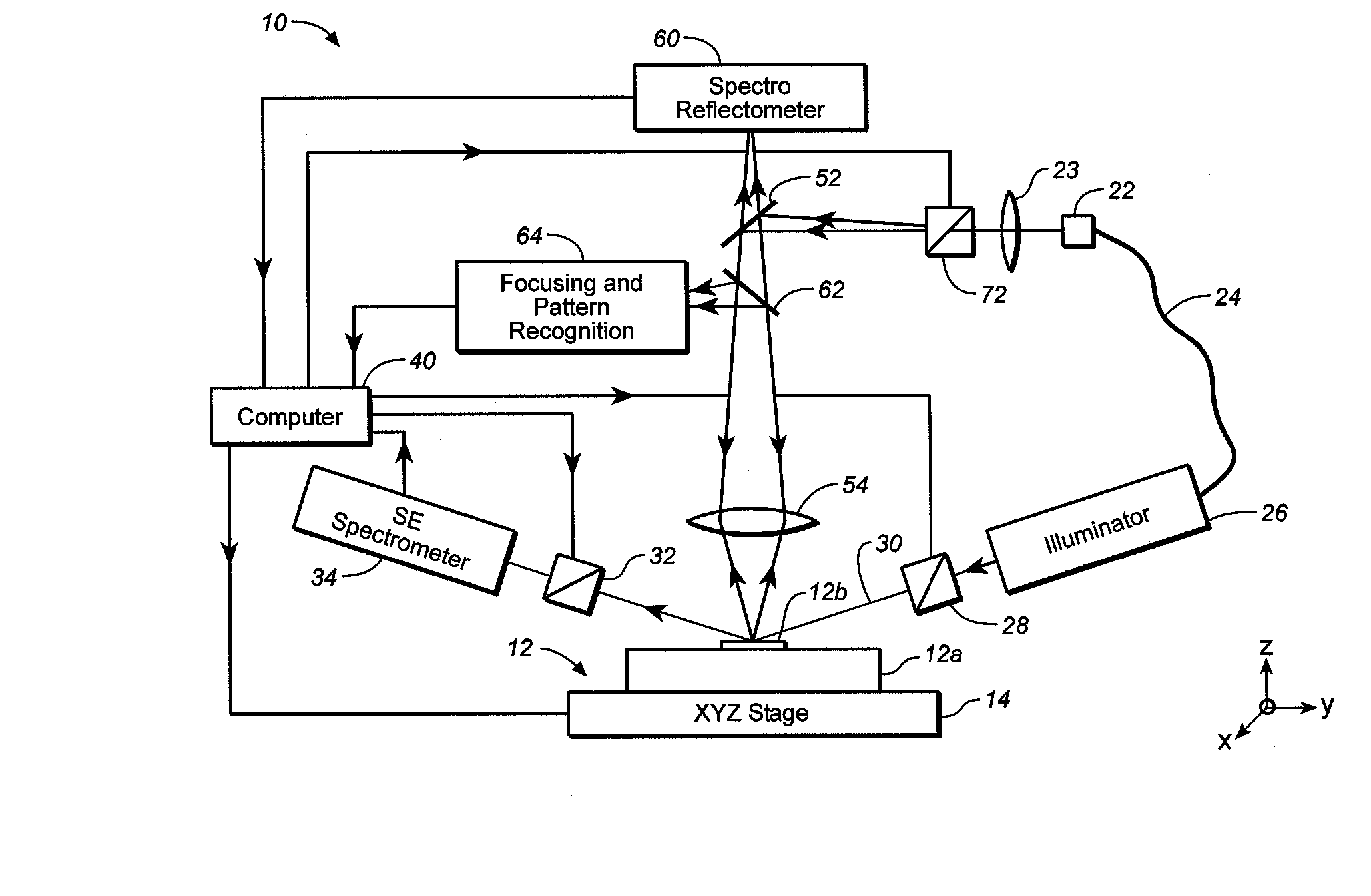
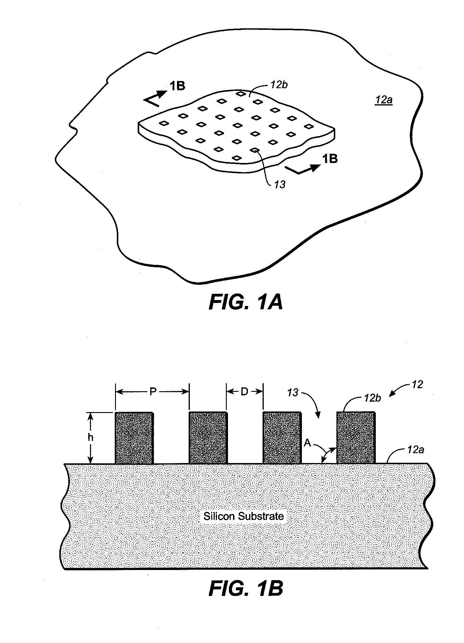
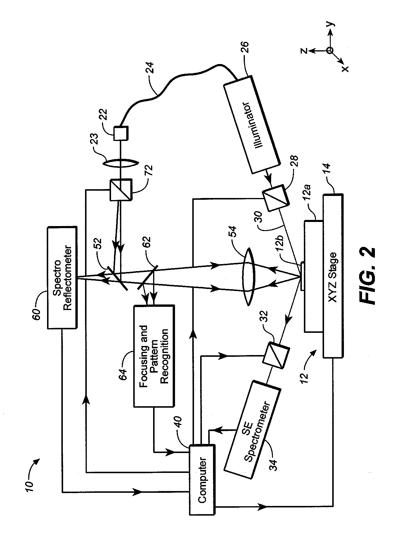
[0018]FIG. 1A is a perspective view of a portion of a semiconductor wafer 12, having a silicon substrate 12a with a layer 12b thereon having a two-dimensional array of contact holes 13 therein. FIG. 1B is a cross-sectional view of wafer 12 of FIG. 1A along the line 1B-1B in FIG. 1A. The cross-sectional view of FIG. 1B is not drawn to the same scale as that in FIG. 1A. Each of the holes 13 in the array of contact holes has a diameter D and the holes are spaced apart at a pitch P, as shown in FIG. 1B. The layer 12b has a thickness or height of h and the side walls of the contact holes 13 are at an angle A to the top surface of the silicon substrate 12a.

[0019] In the conventional method, in order to be able to determine quantities such as D (the diameter of the holes 13), the pitch P, height or thickness, h, and the wall angle A, or other parameters related to the profile or shape of the contact holes 13, all of the above-referenced parameters, as well as the complex index of refracti...


PUM

PropertyMeasurementUnit
wavelengthsaaaaaaaaaa
hole diameteraaaaaaaaaa
wavelengthsaaaaaaaaaa

Abstract

To measure the critical dimensions and other parameters of a one- or two-dimensional diffracting structure of a film, the calculation may be simplified by first performing a measurement of the thickness of the film, employing a film model that does not vary the critical dimension or parameters related to other characteristics of the structure. The thickness of the film may be estimated using the film model sufficiently accurately so that such estimate may be employed to simplify the structure model for deriving the critical dimension and other parameters related to the two-dimensional diffracting structure.

Description

CROSS-REFERENCE TO RELATED APPLICATION [0001] This application claims the benefit of U.S. Provisional Application No. 60 / 643,711, filed Jan. 12, 2005, entitled “System for Measuring a Sample with a Layer Containing a Periodic Diffracting Structure,” which application is incorporated in its entirety by reference as if fully set forth herein.BACKGROUND OF THE INVENTION [0002] This invention relates, in general, to optical sample measurement systems, and in particular, to a system for measuring a sample with a layer containing a periodic diffracting structure. [0003] In semiconductor wafer processing, or similar applications, one frequently encounters the measurements of the dimensions and / or profiles of structures etched in thin films, such as contact holes etched in a resist film or in a dielectric layer. The conventional method for measuring the dimensions and / or profiles of the structures is by means of a spectroscopic scatterometry or spectroscopic critical dimension measurements ...

Claims


Application Information

Patent Timeline
Patent Type & Authority Applications(United States)
IPC IPC(8): G01N21/00G01J3/28
CPCG01N21/211G01N2021/213G01N21/8422G01J4/00
Inventor BAREKET, NOAHWACK, DANIEL C.ZHAO, GUOHENG
Owner KLA TENCOR TECH CORP
Why Eureka
Try Eureka