Method and apparatus for inspection of wafer and semiconductor device

a technology for semiconductor devices and wafers, applied in semiconductor/solid-state device testing/measurement, optical radiation measurement, instruments, etc., can solve the problems of complex and troublesome ultrasonic inspection, secondary appearance defects of semiconductor chips, and the need for human power for ultrasonic inspection, so as to improve inspection efficiency and remove the “defective” semiconductor chips. , the effect of improving the inspection efficiency

Inactive Publication Date: 2008-02-14
YAMAHA CORP
View PDF4 Cites 8 Cited by
  • Summary
  • Abstract
  • Description
  • Claims
  • Application Information

AI Technical Summary

Benefits of technology

[0023]By performing both of the exterior inspection process end the tape inspection process, it is possible to reliably remove the “defective” semiconductor chips. When the exterior inspection process is performed before the tape inspection process in which the semiconductor chips including cracks and defects of relatively lar

Problems solved by technology

That is, a complex and troublesome operation is necessary in the ultrasonic inspection.
In addition, the ultrasonic inspection needs human power for the maintenance of the ultrasonic probe precipitated in pure water.
Furthermore, due to the immersion of the semiconductor chip in pure water during inspection, the semiconductor chip suffers from secondary appearance defects such as staining due to water content adhered thereto.
Since the semiconductor chip is partially immersed in pure water during inspection, it is very difficult to simultaneously perform inspection on the lower surface and side surfaces (or cut surfaces) of the individually isolated wafer.
This also increases the inspection time.
During dicing, cracks may be formed in the backside of the semiconductor chip produced using the wafer, or the semiconductor chip may be partially defective.
The aforementioned d

Method used


Image

  • Method and apparatus for inspection of wafer and semiconductor device
  • Method and apparatus for inspection of wafer and semiconductor device
  • Method and apparatus for inspection of wafer and semiconductor device

Examples


first embodiment

1. First Embodiment

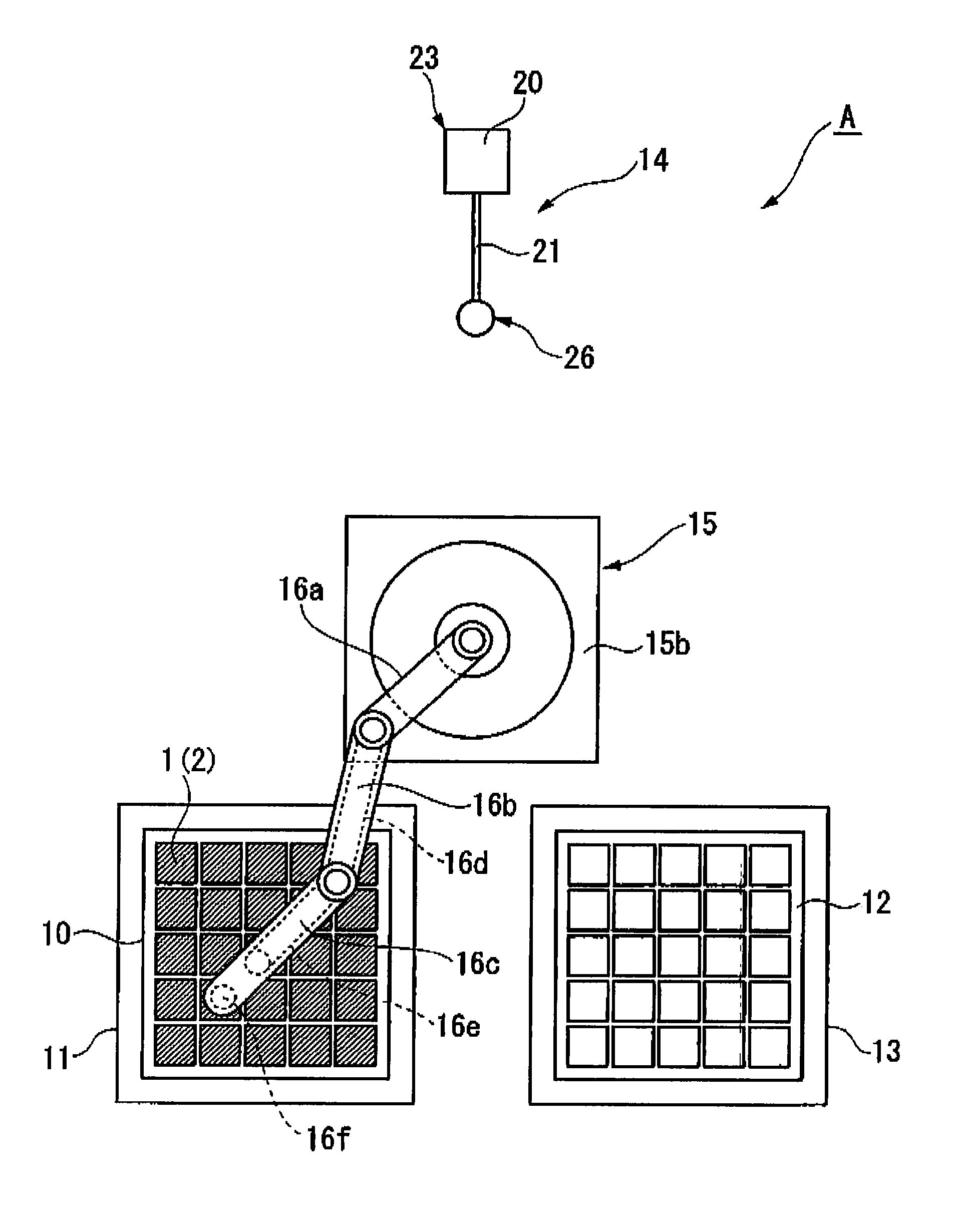
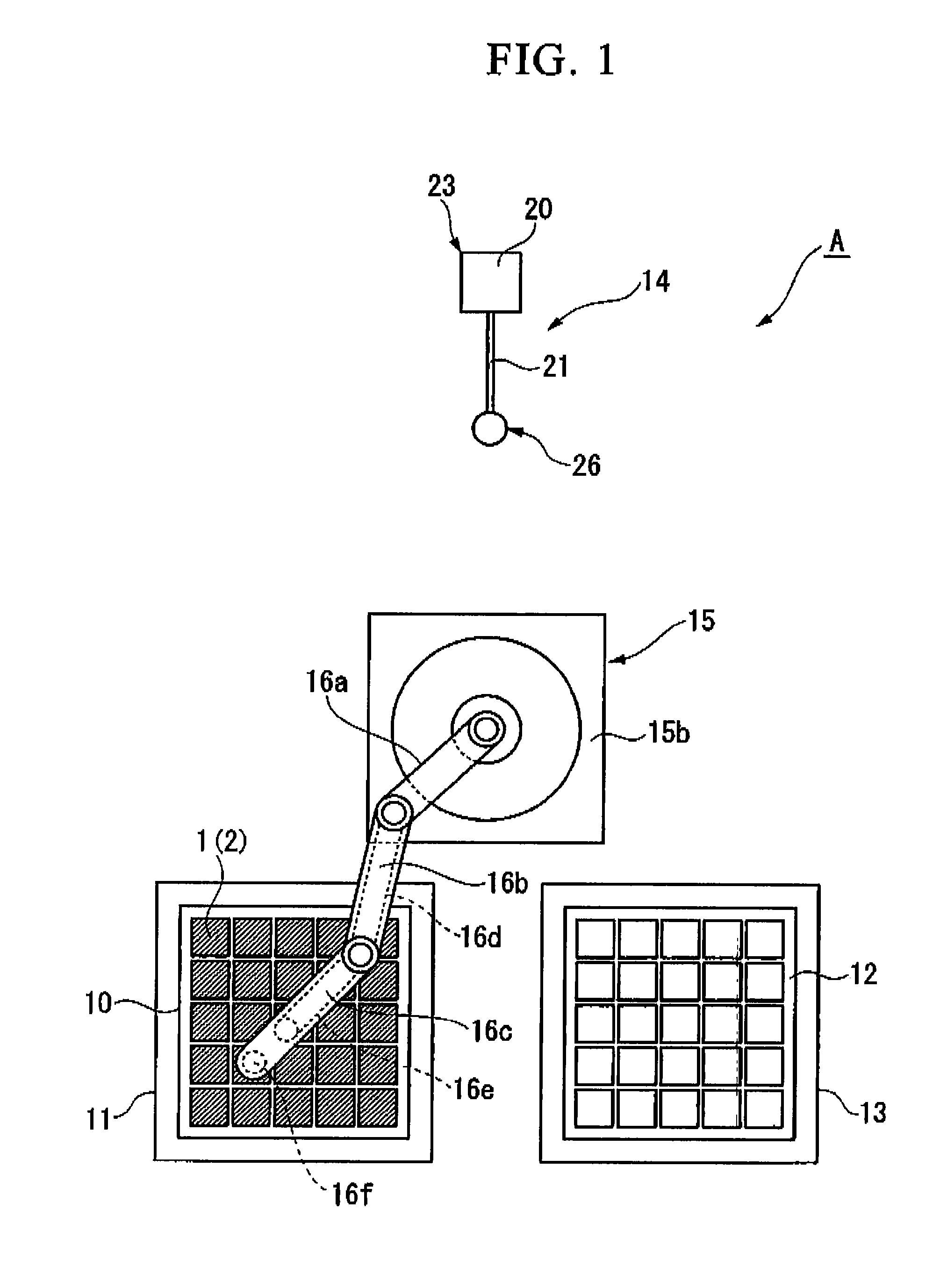
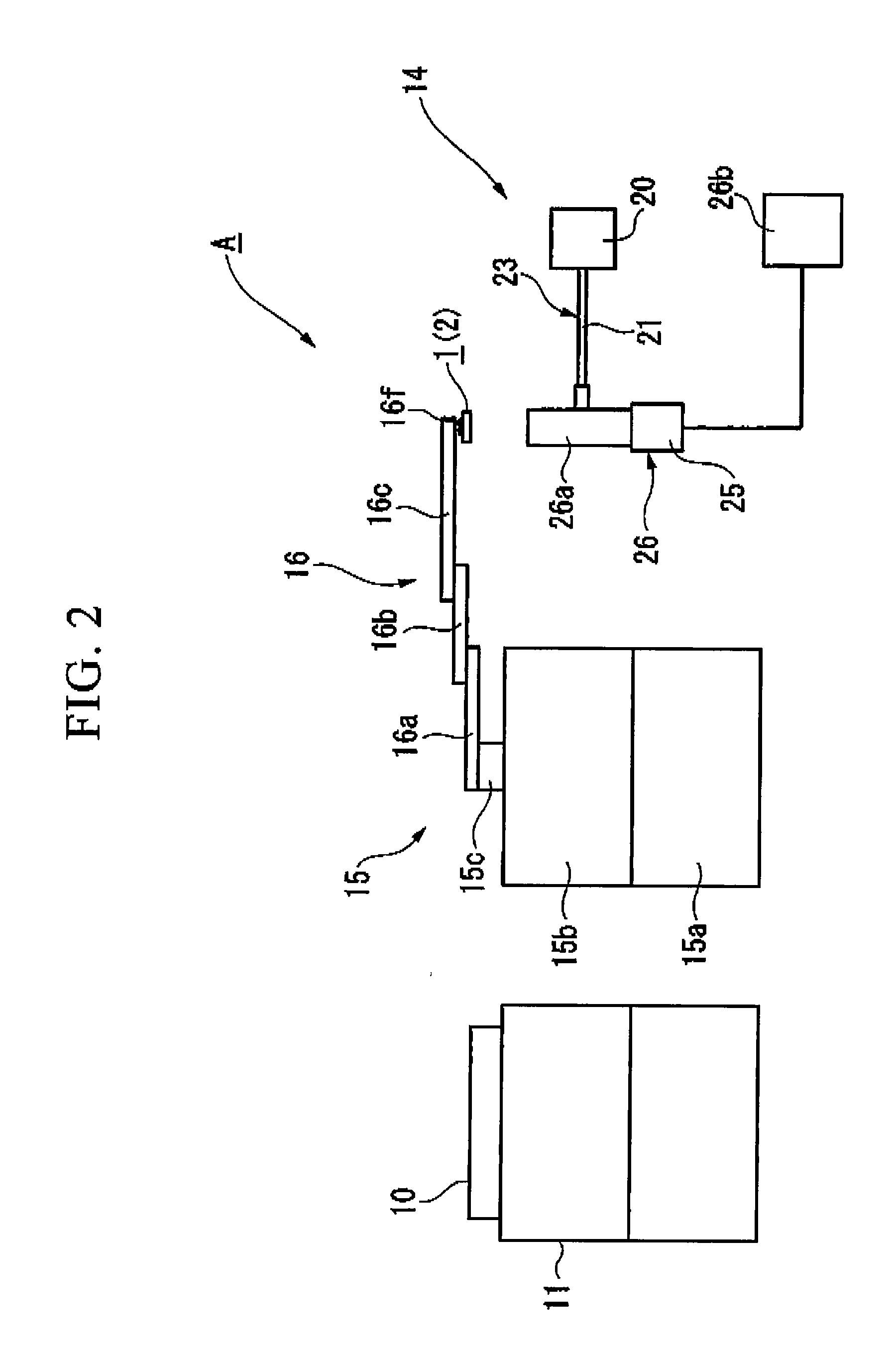
[0044]A method and apparatus for Inspection of a wafer, specifically, for detection of cracks occurring in an individually isolated wafer subjected to dicing, according to a first embodiment of the present invention will be described with reference to FIGS. 1 to 7.

[0045]Specifically, the first embodiment is directed to an inspection method of a wafer 2 forming a semiconductor chip 1 encapsulated in a wafer level chip size package (WL-CSP) and a crack inspection apparatus A of the wafer 2. Herein, an IC 3, a pad electrode 4, a re-wire 5 electrically connected to the IC 3 via the pad electrode 4, and an electrode terminal (i.e., a metal post) 6 are formed on a surface 2a of the wafer having a disk-like shape, which is composed of polycrystal silicon or monocrystal silicon, wherein resin sealing (i.e., formation of a resin layer 7) for protecting the IC 3 from heat, light exposure, and physical impact, and wherein in the last stage of manufacturing, the wafer 2 is su...

second embodiment

2. Second Embodiment

[0071]An inspection method for semiconductor chips according to a second embodiment of the present invention will be described with reference to FIGS. 12 to 18. As shown in FIGS. 12 and 13, a plurality of semiconductor chips 101 subjected to inspection are produced by way of a wafer 103 having a disk-like shape composed of polycrystal silicon or monocrystal silicon.

[0072]A plurality of ICs 105, pad electrodes 107, re-wires 109 electrically connected to the ICs 5 via the pad electrodes 107, electrode terminals (or metal posts) 111, and resin layers 113 to protect the ICs 105 from heat, light radiation, and physical impacts are formed on a surface 103a of the wafer 103. Then, the wafer 103 is subjected to cutting (or dicing) using a thin grindstone having a disk-like shape along dicing lines (or cutting lines) on the surface 103a, thus individually isolating a plurality of semiconductor chips 101.

[0073]In the aforementioned dicing process, a dicing tape 119 (i.e., ...


PUM


Abstract

An individually isolated wafer adapted to a semiconductor chip is subjected to inspection in which an infrared ray is irradiated onto the backside of the wafer whose surface is sealed with a resin layer such that the optical axis thereof perpendicularly or slantingly crosses the surface of the wafer, whereby an image clearly showing cracks formed in lie wafer is produced based on the reflected ray. Before or after an exterior inspection process, a tape inspection process is performed by use of an image of the surface of a dicing tape, in which a plurality of semiconductor chips are once attached onto and then separated from, so as to detect at least one of a defective element, a crack mark, and a foreign mark with regard to the semiconductor chip subjected to inspection,

Description

BACKGROUND OF THE INVENTION[0001]1. Field of the Invention[0002]The present invention relates to methods and apparatuses for inspection of wafers, in particular for detection of cracks formed in wafers during dicing. The present invention also relates to methods for inspection of cracks and defects formed in semiconductor devices during manufacturing.[0003]This application claims priority on Japanese Patent Application No. 2006-220898 and Japanese Patent Application No. 2006-277490, the contents of which are incorporated herein by reference.[0004]2. Description of the Related Art[0005]Due to recent developments of electronic devices such as portable terminals in terms of multiple functions and highly sophisticated functions, it is strongly demanded that semiconductor chips for use in electronic devices be downsized and reduced in thickness and be capable of performing high-speed processing. To meet such demands, semiconductor chips encapsulated in housings such as WL-CSP (i.e., Wafe...

Claims


Application Information

Patent Timeline
IPC IPC(8): G06K9/00G01N21/88
CPCG01N21/9505G01N21/9501H01L22/00
Inventor OHKURA, YOSHIHIROFUKUDA, YOSHIO
Owner YAMAHA CORP
Why Eureka
Try Eureka