Electric fuse circuit and electronic component

a fuse circuit and electronic component technology, applied in the direction of semiconductor devices, semiconductor/solid-state device details, instruments, etc., can solve the problems of insufficient reliability, inability to properly perform writing, and inability to radiate laser beam ls after packaging, etc., to achieve high reliability

Inactive Publication Date: 2008-02-21
FUJITSU MICROELECTRONICS LTD
View PDF16 Cites 16 Cited by
  • Summary
  • Abstract
  • Description
  • Claims
  • Application Information

AI Technical Summary

Benefits of technology

[0014]The objective of the present invention is to provide a h

Problems solved by technology

However, a laser beam LS cannot be radiated after packaging.
Because of a small current supply capacity (approximately several dozen microamperes) of a voltage-boost pumping circuit, which is provided in the semiconductor chip and generates eight-volt VRR, the occurrence of a GIDL current of several hundreds of microamperes prevents the voltage-boost pumping circuit from generating such a high voltage as 8 V; thus, it has been a problem that writing cannot be properly performed.
In addition, it is known that, after the insulating films have been broken, there is a large variation in the resistance values of electric fuses, and therefore, it is not ensured that there would not be a situation where “even though writing has been completed, a detection circuit cannot determine that the el

Method used


Image

  • Electric fuse circuit and electronic component
  • Electric fuse circuit and electronic component
  • Electric fuse circuit and electronic component

Examples


embodiment 1

[0050]FIG. 27 is a diagram illustrating an exemplary configuration of a semiconductor memory chip according to Embodiment 1 of the present invention. An electric fuse circuit 1501, which is a nonvolatile ROM for storing the address of a defective memory cell in a normal memory cell array 1503, outputs the address of the defective memory cell to an address comparator 1502. The address comparator 1502 compares the address of the defective memory cell with an inputted address and then outputs the result of the comparison of the two addresses to the normal memory cell array 1503 and a redundant memory cell array 1504. In the case where the two addresses do not coincide with each other, the normal memory cell array 1503 reads data DQ from or writes the data DQ in the memory cell corresponding to the inputted address. In the case where the two addresses coincide with each other, the redundant memory cell array 1504 reads data DQ from or writes the data DQ in the memory cell corresponding ...

embodiment 2

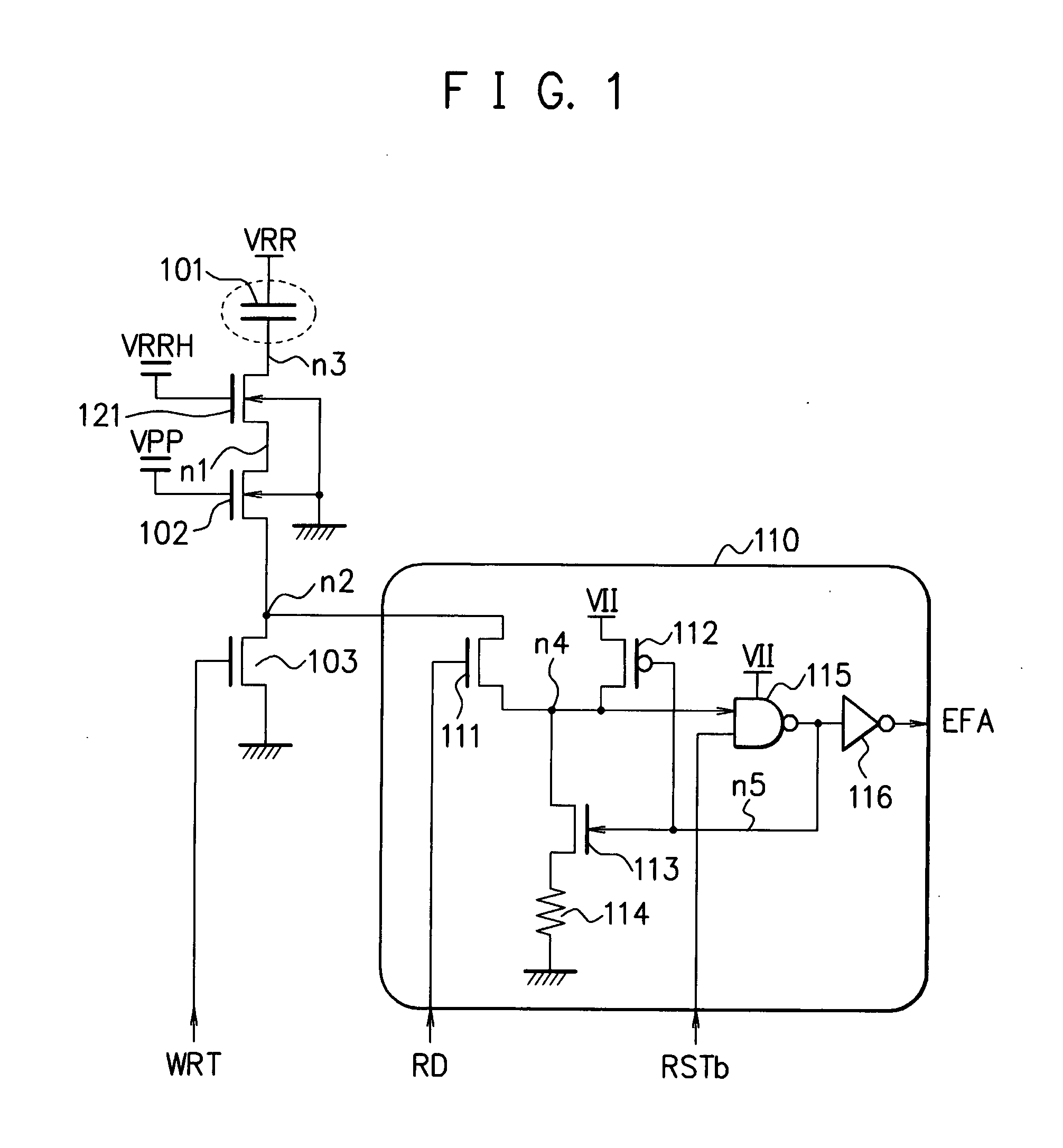
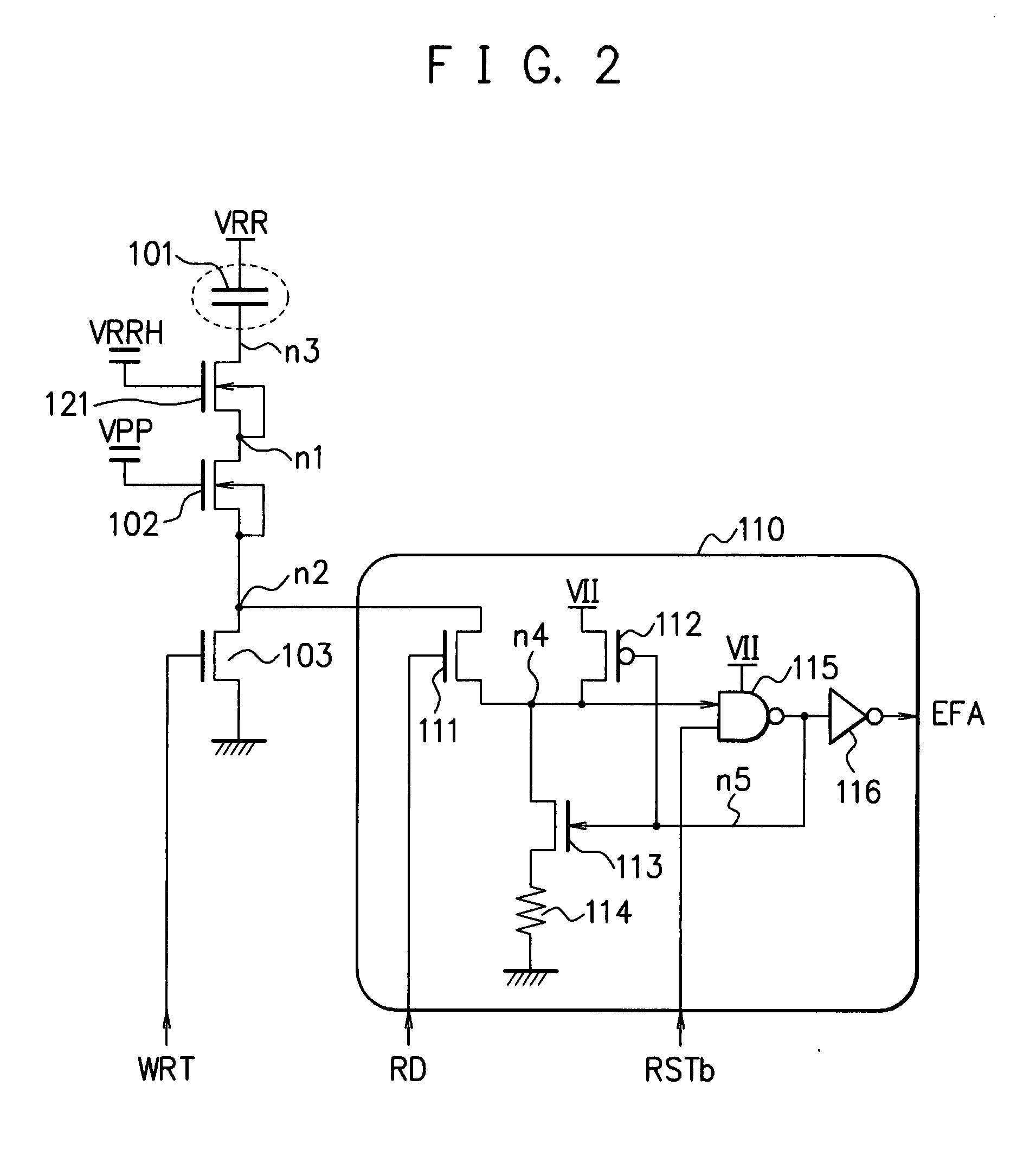
[0065]FIG. 2 is a diagram illustrating an exemplary configuration of an electric fuse circuit 1501 according to Embodiment 2 of the present invention. In contrast to FIG. 1, in FIG. 2, the respective back gates of the transistors 102 and 121 are connected to positions different from those in FIG. 1. In FIG. 1, the respective back gates of the transistors 102 and 121 are connected to the ground. Accordingly, when 8 V is applied to the drain node n3 of the transistor 121, the electric-potential difference between the back gate and the drain node n3 is 8−0=8 V, i.e., a high voltage; thus, the PN junction may be broken.

[0066]In the present embodiment (in FIG. 2), the back gate of the transistor 121 is connected to the source node n1. The back gate of the transistor 102 is connected to the source node n2. When, through writing, the capacitor 101 becomes conductive, the drain node n3 of the transistor 121 becomes 8 V. Because the gate voltage VRRH of the transistor 121 is 5.5 V, the sourc...

embodiment 3

[0068]FIG. 3 is a diagram illustrating an exemplary configuration of the electric fuse circuit 1501 according to Embodiment 3 of the present invention. In the present embodiment, the structural examples of the transistors 102, 103, and 121, and the capacitor 101 will be described. In FIG. 3, the upper part illustrates a circuit diagram; the lower part illustrates a vertical cross-sectional view of the semiconductor substrate corresponding to the circuit diagram. The capacitor 101 is composed of a p-channel transistor. The gate of the p-channel transistor 101 is connected to the node n3, and the source, the drain, and the back gate are connected to the voltage VRR.

[0069]A p-channel substrate 301 is connected to the reference electric potential (ground) VSS. On the p-channel substrate 301, the transistors 101 to 103 and 121 are formed. The source S and the drain D of the transistor 103 are n-channel diffusion regions formed in the p-channel substrate 301. The gate G, the source S, and...


PUM


Abstract

An electric fuse circuit is provided which has a capacitor that forms an electric fuse; a write circuit for breaking an insulating film of the capacitor, by applying a voltage to a terminal of the capacitor in response to a write signal; and at least two transistors, including a first transistor and a second transistor, which are connected in series between the capacitor and the write circuit.

Description

CROSS-REFERENCE TO RELATED APPLICATIONS[0001]This application is based upon and claims the benefit of priority from the prior Japanese Patent Application No. 2006-223428, filed on Aug. 18, 2006, the entire contents of which are incorporated herein by reference.BACKGROUND OF THE INVENTION[0002]1. Field of the Invention[0003]The present invention relates to an electric fuse circuit and an electronic component.[0004]2. Description of the Related Art[0005]FIG. 28 is a view illustrating a semiconductor memory chip having laser fuses. In a recent semiconductor memory, which has a redundant memory cell utilizing a laser fuse, it is common practice to replace a defective memory cell with the redundant memory cell. A laser fuse is a nonvolatile ROM in which information is written by irradiating a laser beam onto a wiring conductive layer to disconnect the fuse (e.g., when being connected, it is electrically conductive, i.e., “0”; when being disconnected, it is electrically nonconductive, i.e...

Claims


Application Information

Patent Timeline
IPC IPC(8): H01L29/00
CPCG11C17/18G11C17/16H01L2224/48137H01L2224/49175H01L2924/00H01L21/82
Inventor YAMAGUCHI, SHUSAKU
Owner FUJITSU MICROELECTRONICS LTD
Why Eureka
Try Eureka