

Semiconductor memory device
a memory device and semiconductor technology, applied in semiconductor devices, digital storage, instruments, etc., can solve the problems of increasing the tip size and thus the production cost and achieve the effect of effective performance of the semiconductor memory devi
- Summary
- Abstract
- Description
- Claims
- Application Information
AI Technical Summary
Benefits of technology
Problems solved by technology
Method used
Image

Examples
first embodiment
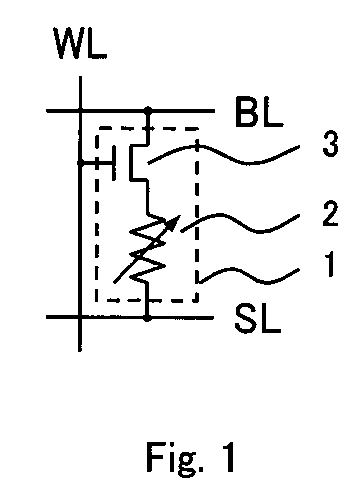
[0061]FIG. 1 schematically illustrates an arrangement of a memory cell provided in the inventive device of the first embodiment. As shown in FIG. 1, the memory cell 1 is of 1T1R type where a variable resistance element 2 is connected in series to a cell access transistor 3. The variable resistance element 2 is a two-port structure type nonvolatile semiconductor memory device arranged for, when receiving a first write voltage between the two ports, shifting its electrical resistance level from a first state to a second state and when receiving between the two ports a second write voltage which is opposite in the polarity to and different in the absolute value from the first write voltage, shifting the electrical resistance level from the second state to the first state thus to store information. The cell access transistor 3 is an n-channel MOSFET of enhancement type which is identical to a MOSFET constituting a peripheral circuit of the memory cell array, which will be described late...
second embodiment
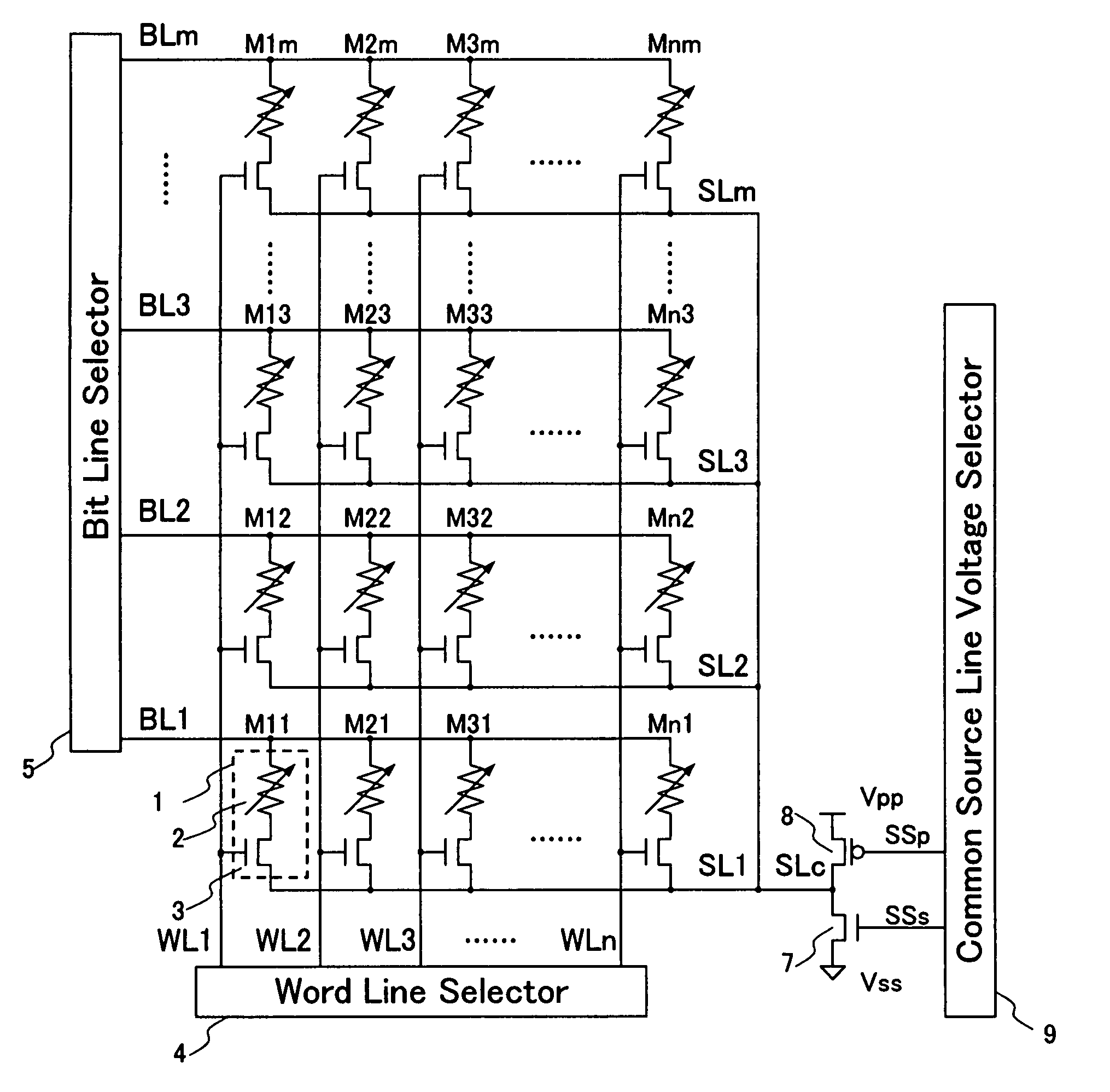
[0079]FIG. 5 schematically illustrates an arrangement of a memory cell array in the second embodiment of the inventive device. The memory cell in the second embodiment is substantially identical in the arrangement to that of the first embodiment shown in FIG. 1. The arrangement of the memory cell array shown in FIG. 5 is also equal to that of the memory cell array of the first embodiment shown in FIG. 2, except for the connection of the source lines. The connection of the source lines will only be described while the explanation of the other common arrangement is omitted. Like components in the memory cell array shown in FIG. 5 are denoted by like numerals as those in the memory cell array shown in FIG. 2 and will be described in no more detail.
[0080]The memory cell array shown in FIG. 5 is arranged in which the source lines SL1 to SLm extending in parallel along the columns are connected to a common source line SLc. The common source line SLc is in turn connected with a pair of an ...
third embodiment
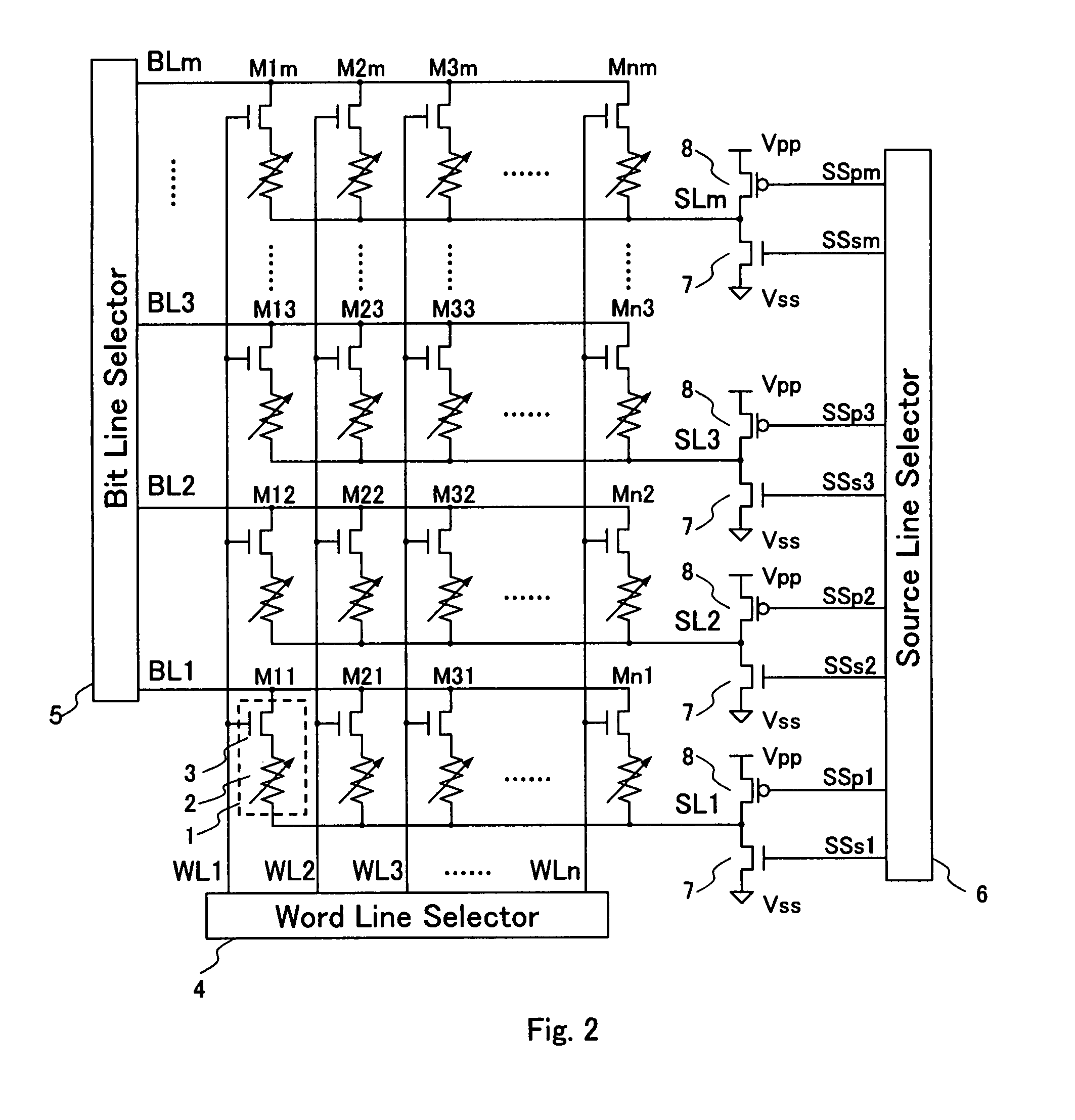
[0091]FIG. 6 schematically illustrates an arrangement of a memory cell array in the third embodiment of the inventive device. The memory cell in the third embodiment is substantially identical in the arrangement to that of the first embodiment shown in FIG. 1. The memory cell array shown in FIG. 6 is also equal in the arrangement of electrical equivalent circuit to but smaller in the layout area than the memory cell array of the second embodiment shown in FIG. 5.
[0092]As shown in FIG. 6, the memory cell array in the third embodiment is arranged in which one source line is commonly provided between any two adjacent columns. Accordingly, the source line extends along and between any two adjacent bit lines (in the horizontal direction shown in FIG. 6) and the number of the source lines in the memory cell array can be decreased to a half as compared with that in the second embodiment.
[0093]FIG. 7 schematically illustrates a plan view of the memory cell array shown in FIG. 6. In FIG. 7, ...
PUM
 Abstract
Description
Claims
Application Information