
Data output apparatus, memory system, data output method, and data processing method

Inactive Publication Date: 2008-03-06
CANON KK
View PDF7 Cites 15 Cited by
  • Summary
  • Abstract
  • Description
  • Claims
  • Application Information

AI Technical Summary

Benefits of technology

[0013]The present invention provides a technique that reduces noise when writing data in a memory or reading out data from a memory.

Problems solved by technology

The increase in operating frequency has also increased the electromagnetic radiation of an LSI, and makes it difficult to control EMI (Electro Magnetic Interference).
When a transistor on an LSI chip switches, a high-frequency electric current flows through a power supply / ground line and generates noise on it.
This noise increases in proportion to the number of transistors that switch.
The noise increases as the operating frequency and integration degree of an LSI increase.
On the other hand, the noise margin decreases as the power supply voltage of an LSI lowers and its operating frequency increases.
Unfortunately, the memory access signal generator described in Japanese Patent Laid-Open No. 2004-213563 has the problem that if the number of times of data switching increases, noise increases, and the noise decreases the operation margin.

Method used


Image

  • Data output apparatus, memory system, data output method, and data processing method
  • Data output apparatus, memory system, data output method, and data processing method
  • Data output apparatus, memory system, data output method, and data processing method

Examples


first embodiment

[0037]Embodiments of the present invention will be explained in detail below with reference to the accompanying drawings. Note that the following embodiments do not limit the present invention according to the scope of claims. Note also that not all combinations of features explained in the embodiments are essential to the means of the present invention.

[0038]First, a memory system according to the first embodiment of the present invention will be explained.

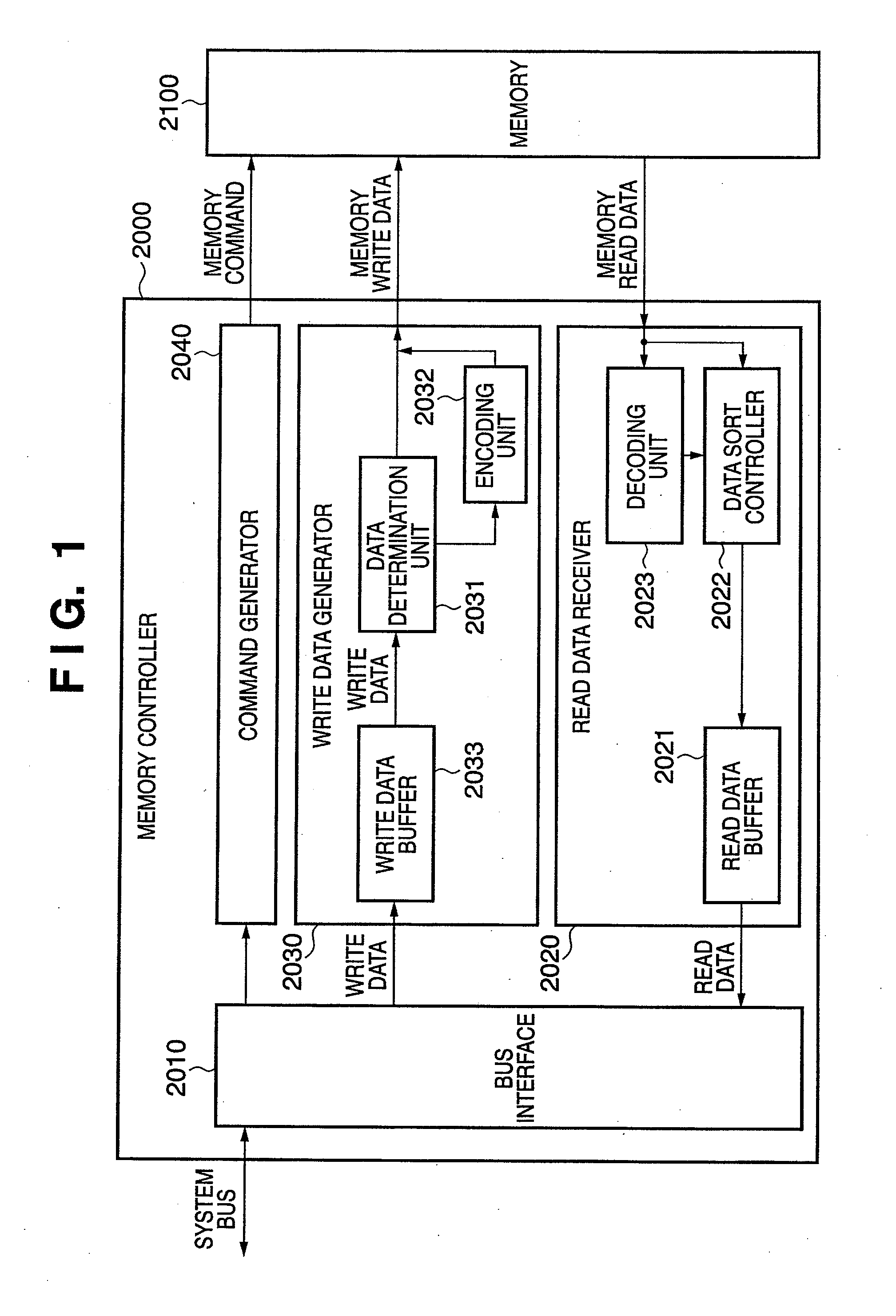
[0039]FIG. 1 shows the memory system according to this embodiment.

[0040]In FIG. 1, reference numeral 2000 denotes a memory controller; and 2100, a memory. The memory controller 2000 includes a bus interface 2010, command generator 2040, write data generator 2030, and read data receiver 2020.

[0041]The write data generator 2030 comprises a write data buffer 2033, data determination unit 2031, and encoding unit 2032. The read data receiver 2020 comprises a read data buffer 2021, data sort controller 2022, and decoding unit 2023.

[004...

second embodiment

[0062]A memory system according to the second embodiment of the present invention will be explained below.

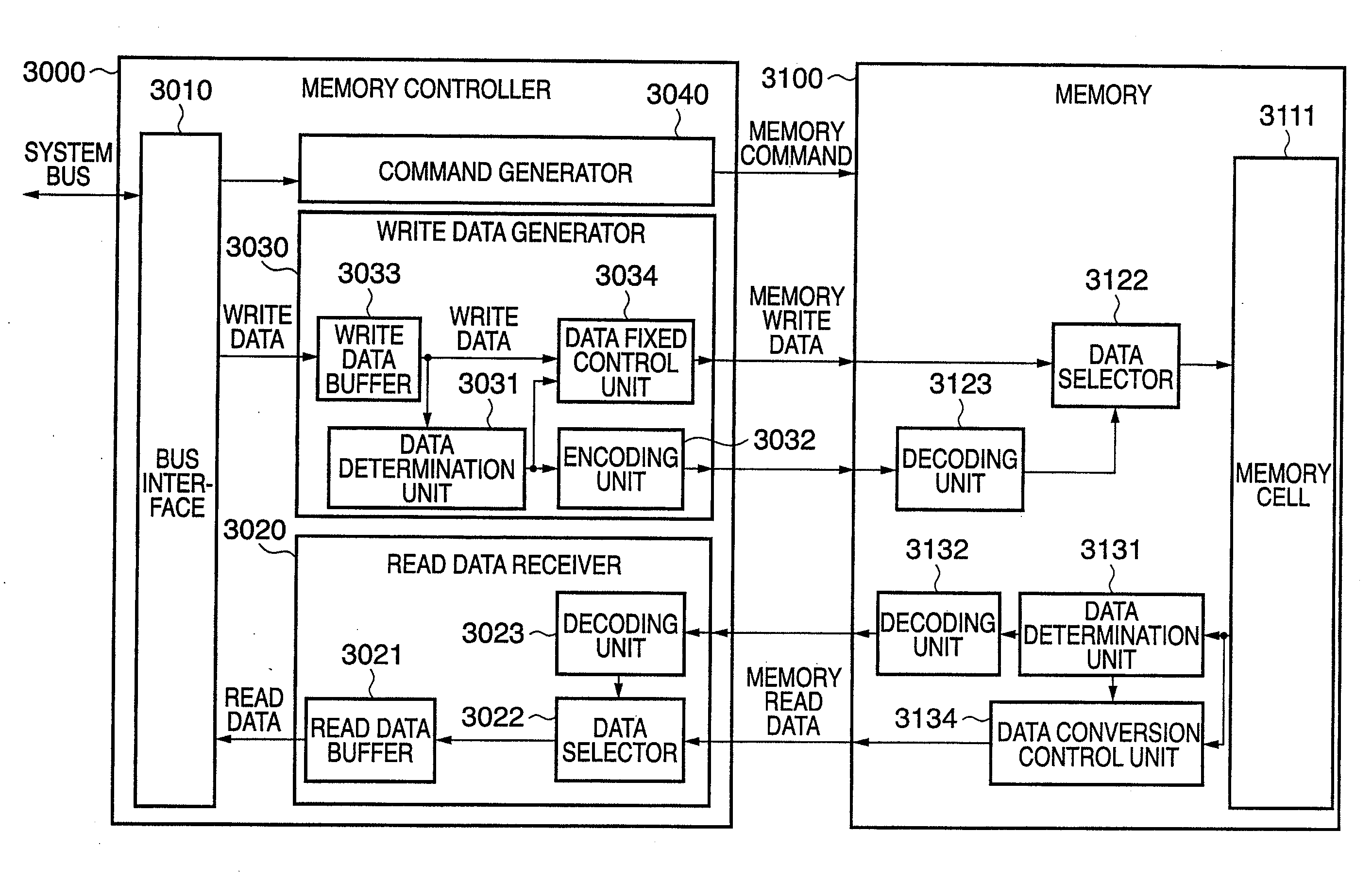
[0063]FIG. 5 shows the memory system according to this embodiment.

[0064]Reference numeral 3000 denotes a memory controller; and 3100, a memory. The memory controller 3000 includes a bus interface 3010, command generator 3040, write data generator 3030, read data receiver 3020, and the like.

[0065]The write data generator 3030 includes a write data buffer 3033, data determination unit 3031, encoding unit 3032, data fixed control unit 3034, and the like. The read data receiver 3020 includes a read data buffer 3021, data selector 3022, decoding unit 3023, and the like.

[0066]The memory controller 3000 having received a write request from a system bus generates a command and write data in accordance with a bus protocol using the bus interface 3010. The memory controller 3000 transmits the command to the command generator 3040, and the write data to the write data generator 3030.

[0067]...

third embodiment

[0086]FIG. 11 is a block diagram showing the arrangement of a memory system according to an embodiment of the present invention.

[0087]In FIG. 11, the same reference numerals as the constituent elements shown in FIG. 5 denote constituent elements given the same names. Reference numeral 3000 denotes a memory controller; and 3100, a memory (memory element) having a memory cell 3111.

[0088]A bus interface 3010 connects an internal bus of the memory controller 3000 and a system bus. A read data receiver 3020 outputs data read out from the memory 3100 to the bus interface 3010. A read data buffer 3021 temporarily holds data readout from the memory 3100 and processed, and outputs the data to the bus interface 3010. A data selector 3022 processes data read out from the memory 3100 as explained in the second embodiment. A decoding unit 3023 decodes encoded data output from an encoding unit 3132 of the memory 3100.

[0089]A write data generator 3030 temporarily stores write data received from th...


PUM


Abstract

A data output apparatus converts input data into data that changes less than the input data, and outputs the converted data to a memory.

Description

BACKGROUND OF THE INVENTION[0001]1. Field of the Invention[0002]The present invention relates to a data output apparatus and method of outputting data to a memory, a memory system having a memory device and memory controller, and a data processing method of the memory device in the memory system.[0003]2. Description of the Related Art[0004]Recently, the improvement of the semiconductor process has dramatically increased the integration degree and operating frequency of an LSI, and the performance of an apparatus using this LSI has also increased. The increase in operating frequency has also increased the electromagnetic radiation of an LSI, and makes it difficult to control EMI (Electro Magnetic Interference). When the operating frequency of an LSI rises, the amount of harmonic components at high frequencies contained in a clock signal increases, and this increases the radiation of the harmonic components.[0005]An SSCG (Spread Spectrum Clock Generator) is used to control the EMI. Th...

Claims


Application Information

Patent Timeline
IPC IPC(8): G11C7/10H03M7/02
CPCG11C7/1006G11C7/02
Inventor SUZUKI, TAKESHIUEDA, KOICHIFUKATSU, TSUTOMU
Owner CANON KK
Learn More