

Process For Fabricating Semiconductor Device
a manufacturing process and semiconductor technology, applied in the direction of coatings, chemical vapor deposition coatings, metallic material coating processes, etc., can solve the problems of deterioration in the reliability of semiconductor devices, deterioration of electrical characteristics, insulation resistance, etc., and achieve the effect of improving electrical characteristics and reliability
- Summary
- Abstract
- Description
- Claims
- Application Information
AI Technical Summary
Benefits of technology
Problems solved by technology
Method used
Image

Examples
Embodiment Construction
[0039] Embodiments of the present invention will now be described with reference to the accompanying drawings. Hereinafter, the present invention is exemplified by a wafer processing system in which a semiconductor device is manufactured by a single damascene method or dual damascene method. Where an interconnection structure is formed by a single damascene method or dual damascene method, an interconnection groove or connection hole (which will be referred to as “interconnection groove or the like” hereinafter) is utilized.
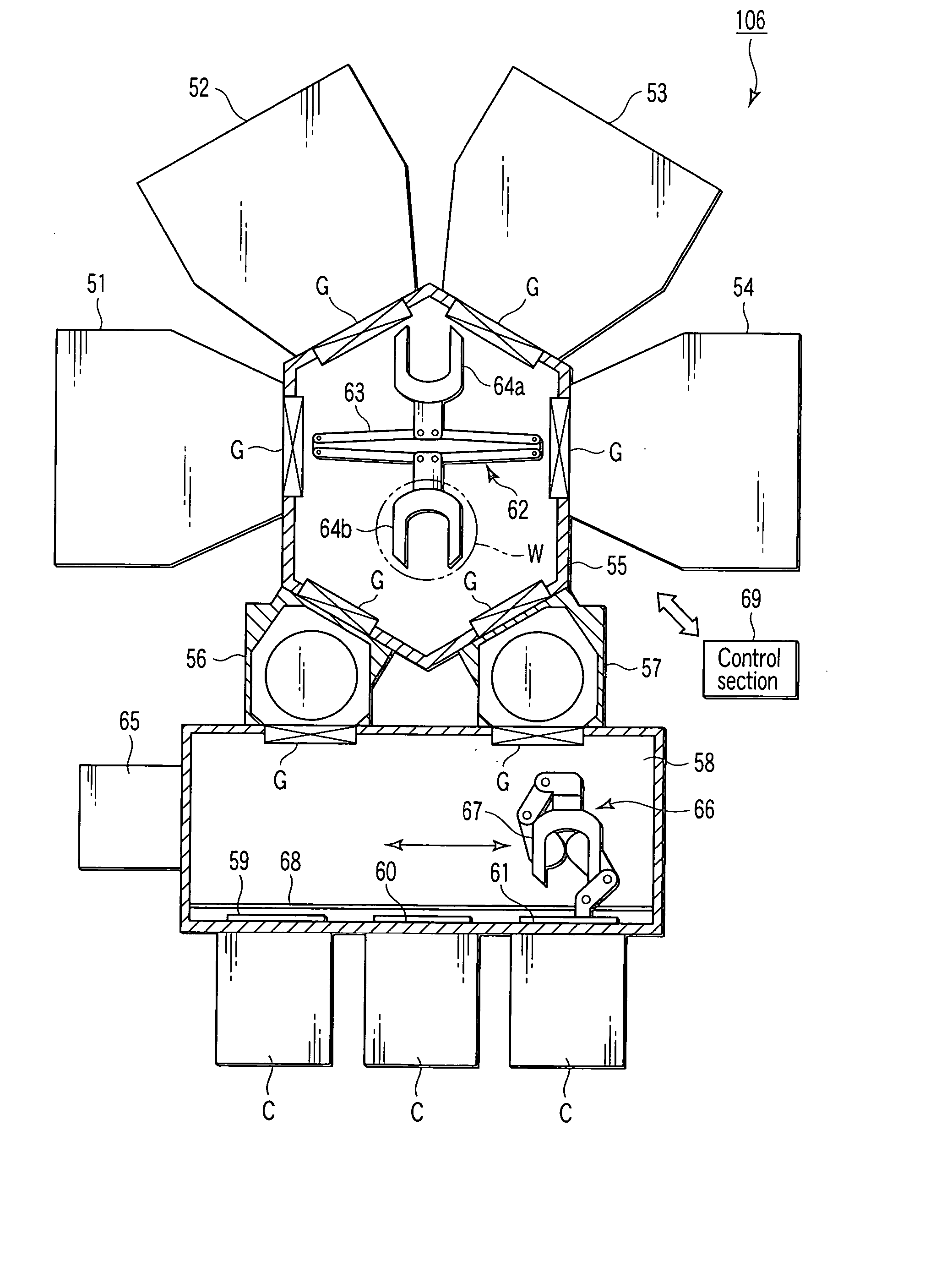
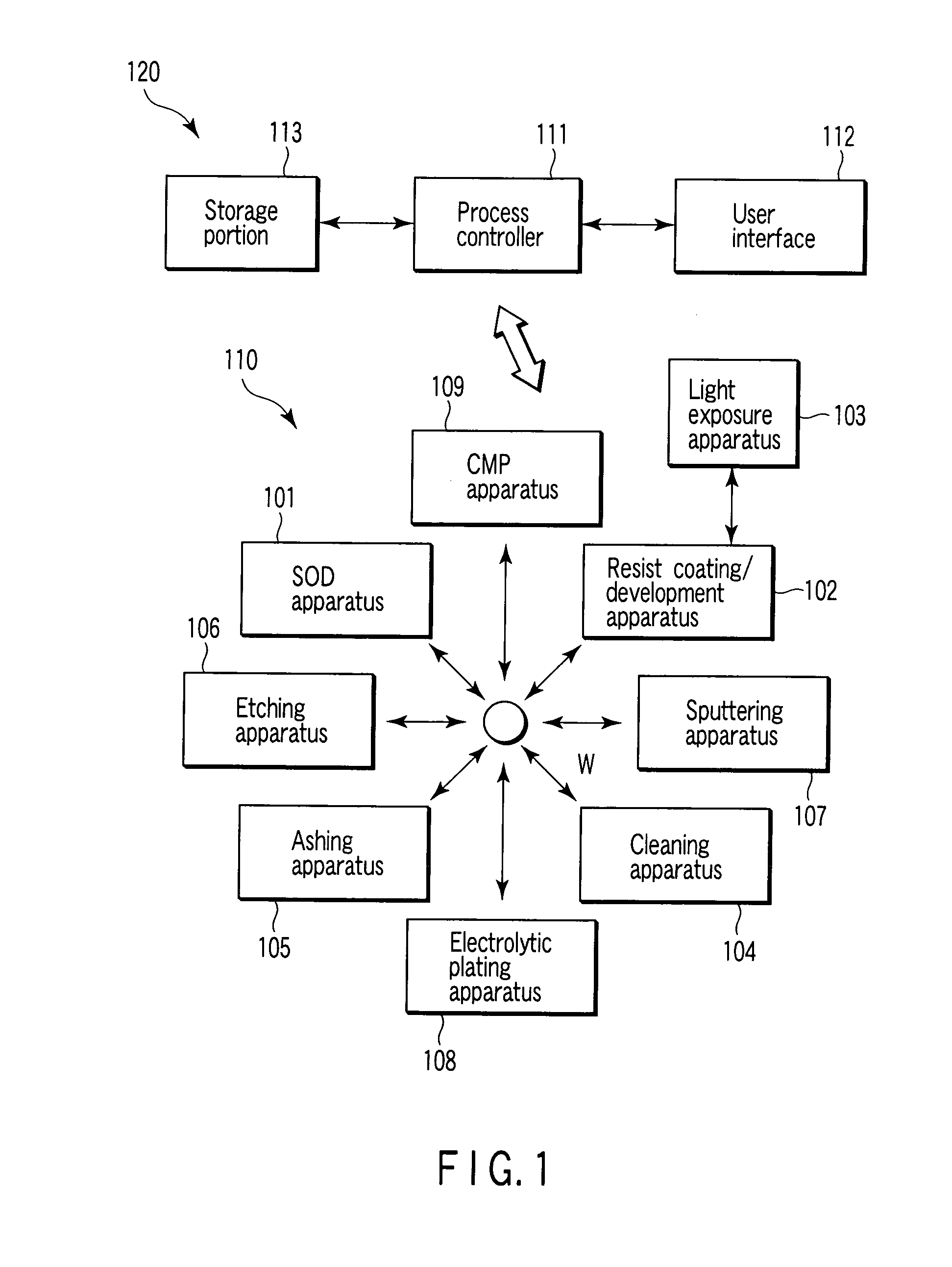
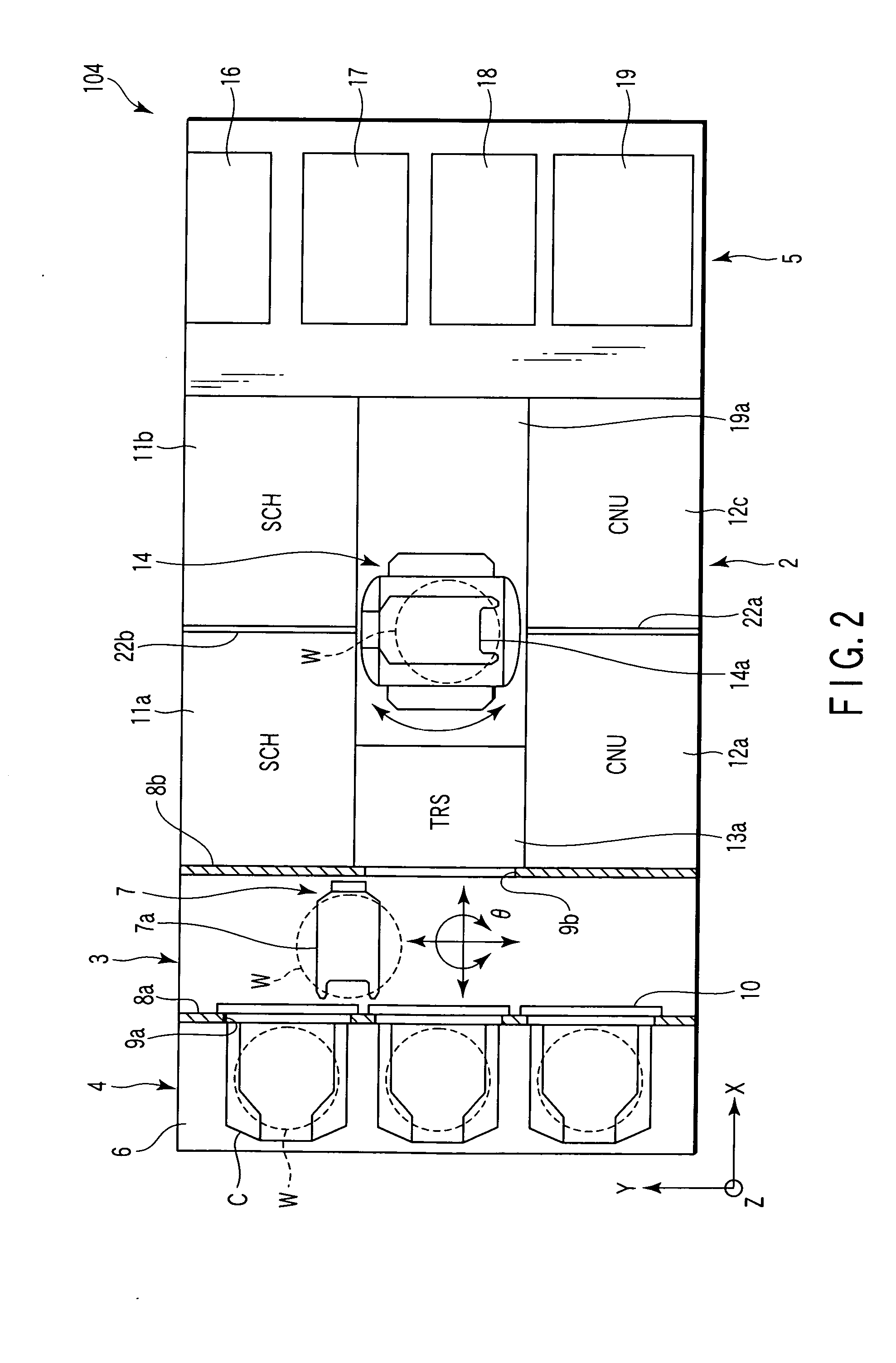
[0040]FIG. 1 is an explanatory view schematically showing the arrangement of a wafer processing system. This wafer processing system includes a process section 110 and a main control section 120. The process section 110 includes an SOD (Spin On Dielectric) apparatus 101, a resist coating / development apparatus 102, a light exposure apparatus 103, a cleaning apparatus 104, an ashing apparatus 105, an etching apparatus 106, a sputtering apparatus 107 used as a PVD ...
PUM
| Property | Measurement | Unit |
|---|---|---|
| temperature | aaaaa | aaaaa |
| temperature | aaaaa | aaaaa |
| flow rate | aaaaa | aaaaa |
Abstract
Description
Claims
Application Information