

Defect Inspection Apparatus and Defect Inspection Method
a technology of defect inspection and inspection apparatus, which is applied in the direction of semiconductor/solid-state device testing/measurement, image enhancement, instruments, etc., can solve the problems of not being able to easily perform high-speed and high-sensitivity detection of defects, sensitivity is considerably reduced on parts, and detection sensitivity (minimum detectable foreign material size) is considerably reduced, so as to improve the defect classification performance and the effect of defect capture ra
- Summary
- Abstract
- Description
- Claims
- Application Information
AI Technical Summary
Benefits of technology
Problems solved by technology
Method used
Image

Examples
first embodiment
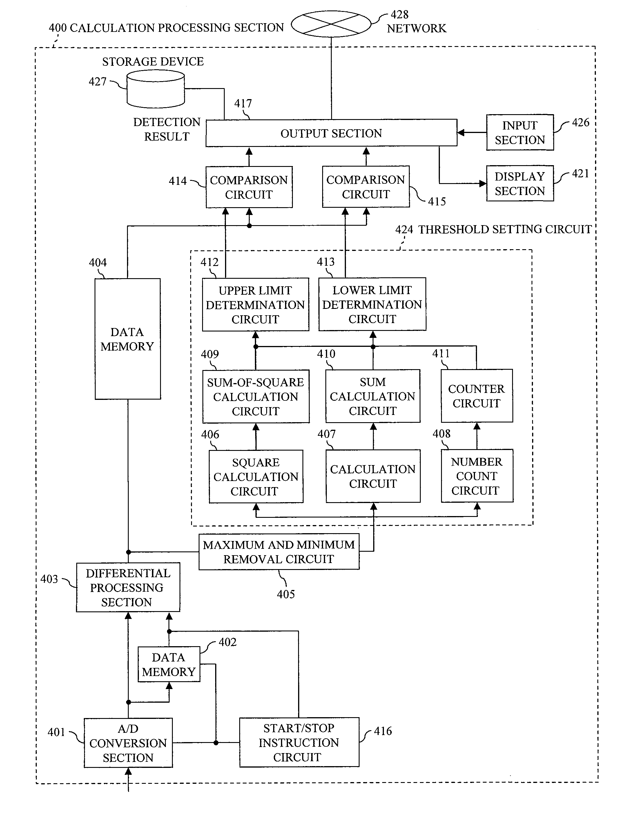
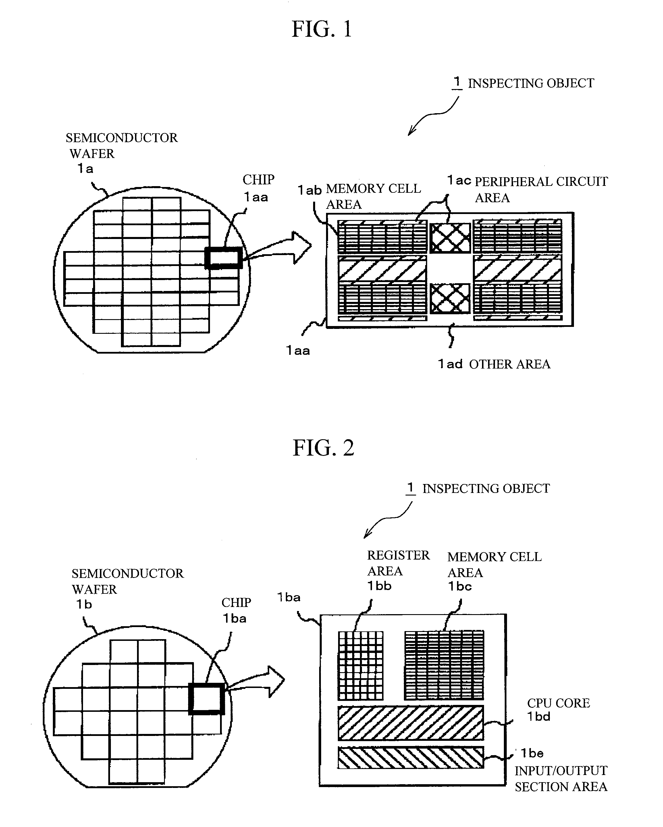
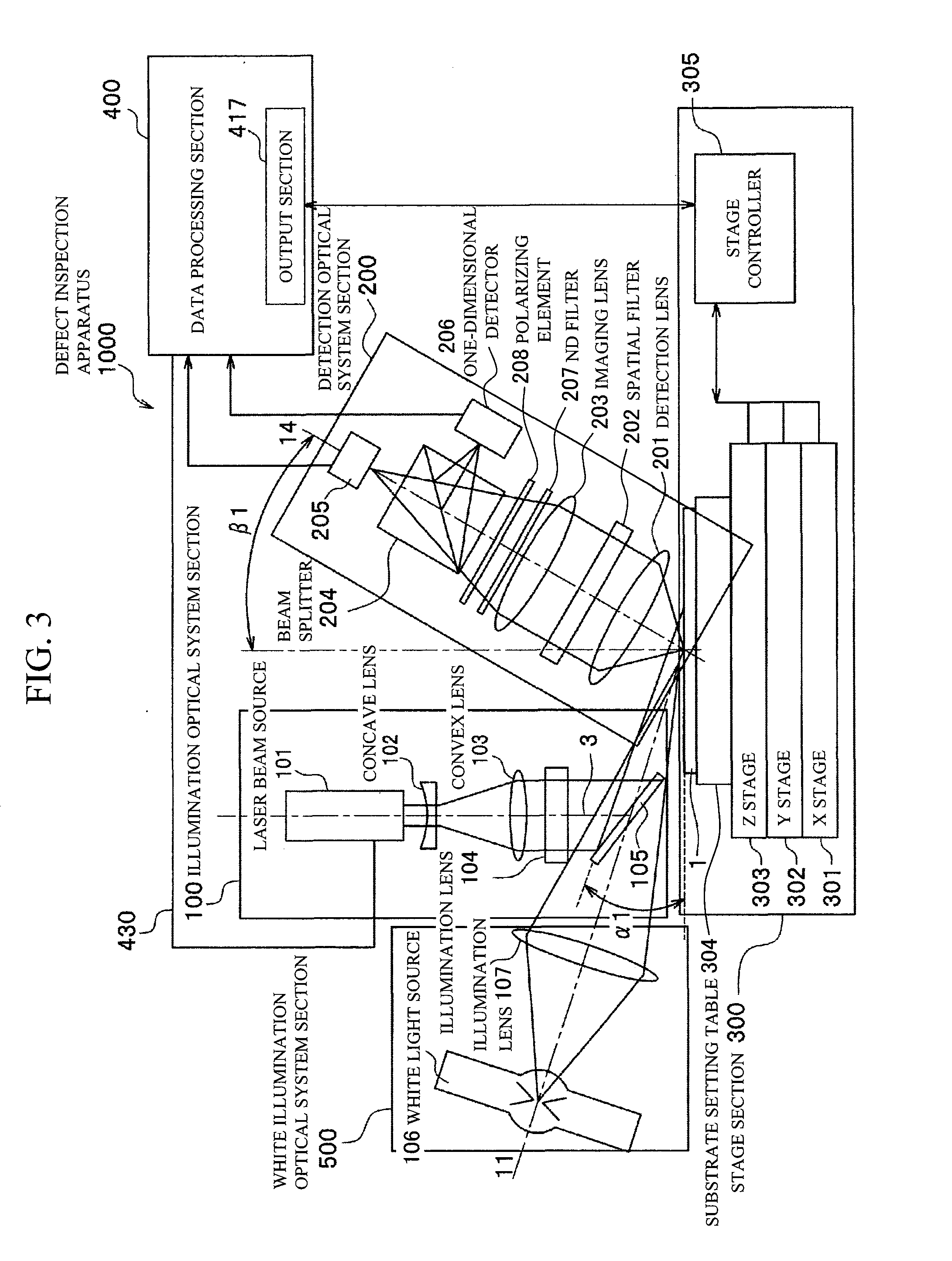
[0037] The defect inspection apparatus according to one embodiment of the present invention illuminates the inspecting object 1 with a laser beam and receives scattered light caused by a defect such as a foreign material existing on a pattern area. In this case, a spatial filter is provided to prevent zero-order diffracted light of a circuit pattern (linear pattern), which is formed of a group of lines parallel to each other on a non-repetition pattern area in the chip, from entering an entrance pupil of an objective lens. At this time, the defect inspection apparatus simultaneously emits light from a direction opposite to the direction of illumination light, and detects both forward-scattered light and backward-scattered light. This allows classification that regards asymmetry of the defect as a characteristic and allows classification between a defect having strong forward scatter and a defect having strong backward scatter.
[0038] Moreover, the defect inspection apparatus detects...
modification example
[0105] The present invention is not limited to the aforementioned embodiment, and, for example, the following modification may be possible.
[0106] (1) Although the laser beam source having a fundamental wave is used as the laser beam source 101 in the aforementioned embodiment, it is possible to use a harmonic laser. For example, a scattering coefficient also depends on an index of refraction, and the semiconductor material includes one whose index of refraction comes close to 1 in a specific wavelength region. FIG. 18 shows wavelength characteristics of complex indexes of refraction (n-jk) of tungsten W and crystallized silicon c-Si. Here, a thick solid line shows a real part n_W of index refraction of tungsten, and a thin solid line shows an imaginary part k_W. Moreover, a thick broken line shows a real part n_c-Si of index refraction of crystallized silicon, and a thin broken line shows an imaginary part k_c-Si. For example, in a short wavelength region in the vicinity of 200 nm,...
PUM
 Abstract
Description
Claims
Application Information