Film formation method and apparatus for semiconductor process

a film formation method and semiconductor technology, applied in the direction of resistive material coating, superimposed coating process, vacuum evaporation coating, etc., can solve the problem of low film thickness controllability of the process, unsuitability of thermal cvd process at high temperature, and inability to meet the requirements of film thickness control, etc. problem, to achieve the effect of high film thickness controllability

Active Publication Date: 2008-03-13
TOKYO ELECTRON LTD
View PDF7 Cites 79 Cited by
  • Summary
  • Abstract
  • Description
  • Claims
  • Application Information

AI Technical Summary

Benefits of technology

[0013] An object of the present invention is to provide a method and apparatus for forming an insulating film, which can employ a relatively low process temperature in film formation, and cause the film to be etched by a low amount during a cleaning process, so that the cleaning process can be perfor

Problems solved by technology

However, where a thin film having a low heat resistance is present as an underlayer, a thermal CVD process at high temperature is unsuitable.
Accordingly, the insulating film may be excess

Method used


Image

  • Film formation method and apparatus for semiconductor process
  • Film formation method and apparatus for semiconductor process
  • Film formation method and apparatus for semiconductor process

Examples


first embodiment

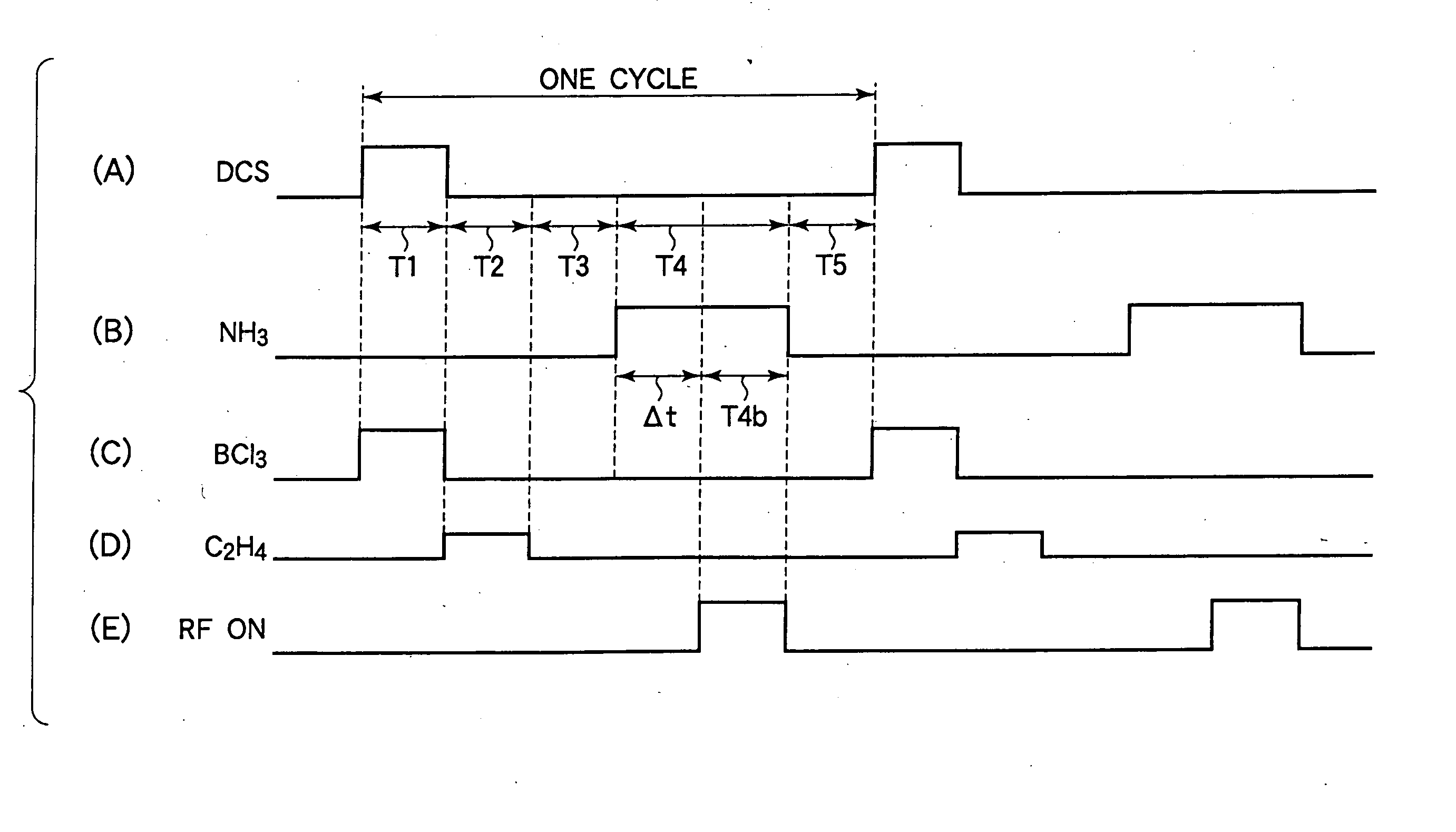
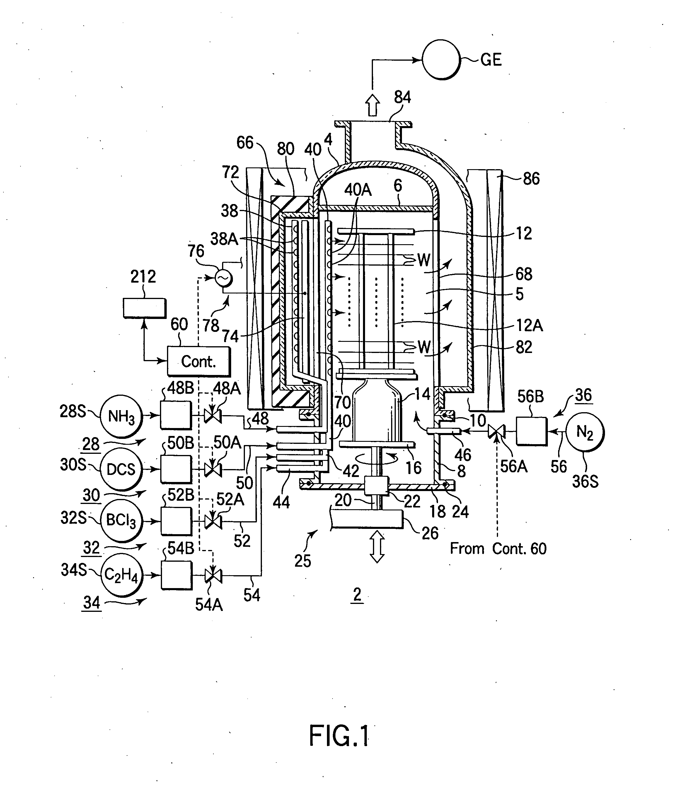
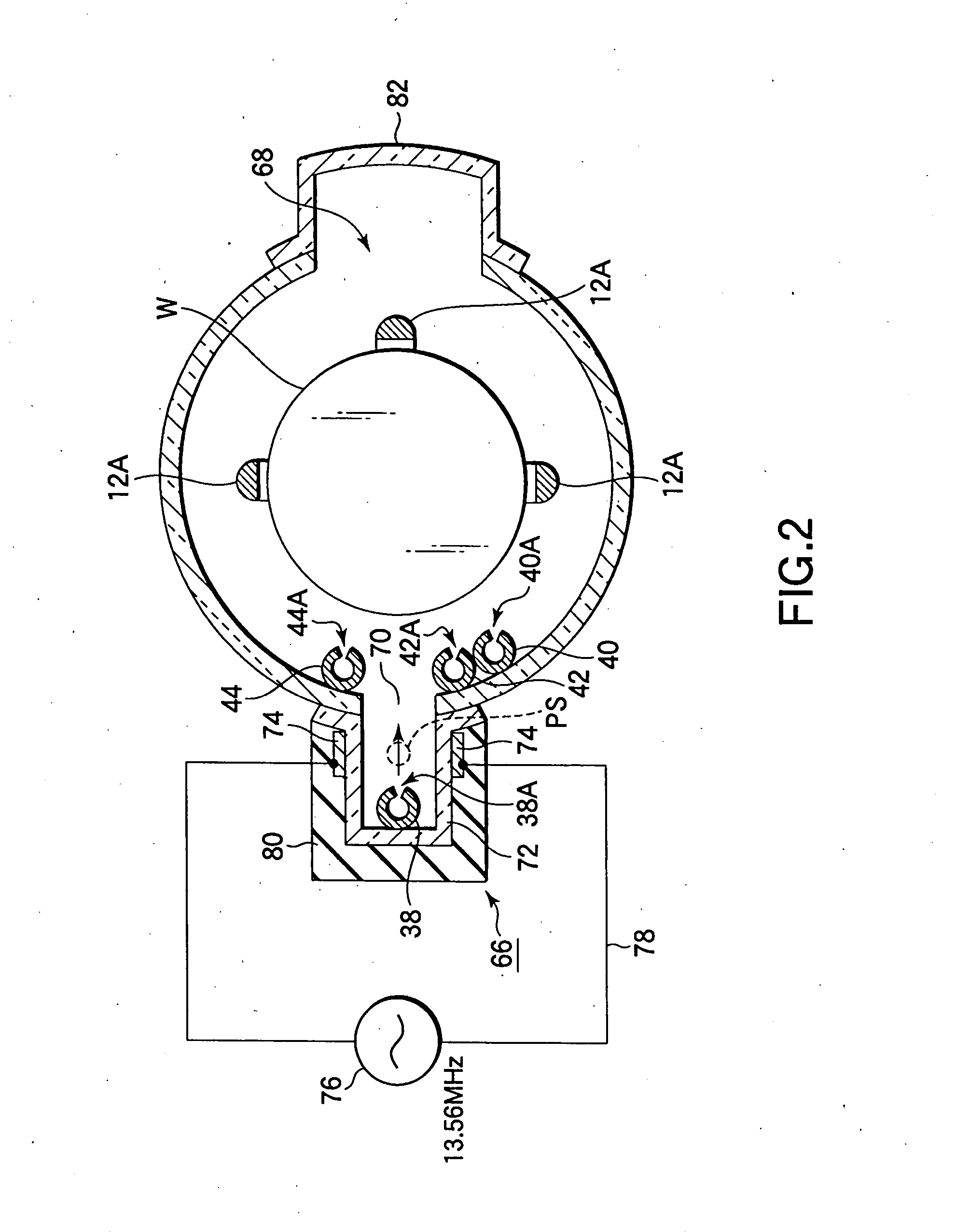
[0053]FIG. 3 is a timing chart of the gas supply and RF (radio frequency) application of a film formation method according to a first embodiment of the present invention. As shown in FIG. 3, the film formation method according to this embodiment is arranged to alternately repeat first to fifth steps T1 to T5. A cycle comprising the first to fifth steps T1 to T5 is repeated a number of times, and thin films of SiBCN formed by respective cycles are laminated, thereby arriving at an SiBCN film having a target thickness.

[0054] Specifically, the first step T1 is arranged to perform supply of the first process gas (denoted as DCS in FIG. 3) and the third process gas (denoted as BCl3 in FIG. 3) to the process field 5, while stopping supply of the second process gas (denoted as NH3 in FIG. 3) and the fourth process gas (denoted as C2H4 in FIG. 3) to the process field 5. The second step T2 is arranged to perform supply of the fourth process gas to the process field 5, while stopping supply ...

second embodiment

[0065]FIG. 4 is a timing chart of the gas supply and RF (radio frequency) application of a film formation method according to a second embodiment of the present invention. As shown in FIG. 4, the film formation method according to this embodiment is also arranged to alternately repeat first to fifth steps T11 to T15. A cycle comprising the first to fifth steps T11 to T15 is repeated a number of times, and thin films of SiBCN formed by respective cycles are laminated, thereby arriving at an SiBCN film having a target thickness.

[0066] Specifically, in the second embodiment, the first, third, fourth, and fifth steps T11, T13, T14, and T15 are set to have exactly the same arrangements as the first, third, fourth, and fifth step T1, T3, T4, and T5 of the first embodiment, respectively. However, unlike the second step T2 of the first embodiment, the second step T12 is arranged to perform supply of the first process gas (denoted as DCS in FIG. 4) and the fourth process gas (denoted as C2H...

third embodiment

[0068]FIG. 5 is a timing chart of the gas supply and RF (radio frequency) application of a film formation method according to a third embodiment of the present invention. As shown in FIG. 5, the film formation method according to this embodiment is also arranged to alternately repeat first to fifth steps T21 to T25. A cycle comprising the first to fifth steps T21 to T25 is repeated a number of times, and thin films of SiBCN formed by respective cycles are laminated, thereby arriving at an SiBCN film having a target thickness.

[0069] Specifically, in the third embodiment, the third, fourth, and fifth steps T23, T24, and T25 are set to have exactly the same arrangements as the third, fourth, and fifth step T3, T4, and T5 of the first embodiment, respectively. However, as compared with the first and second steps T1 and T2 of the first embodiment, the first and second steps T21 and T22 are arranged such that the order of supply of the third process gas (denoted as BCl3 in FIG. 5) and th...


PUM

PropertyMeasurementUnit
Temperatureaaaaaaaaaa
Pressureaaaaaaaaaa
Pressureaaaaaaaaaa

Abstract

An insulating film is formed on a target substrate by CVD, in a process field to be selectively supplied with a first process gas containing a silane family gas, a second process gas containing a nitriding gas or oxynitriding gas, a third process gas containing a boron-containing gas, and a fourth process gas containing a carbon hydride gas. A first step performs supply of the first process gas and a preceding gas, which is one of the third and fourth process gases, while stopping supply of the second process gas and a succeeding gas, which is the other of the third and fourth process gases. A second step performs supply of the succeeding gas, while stopping supply of the second process gas and the preceding gas. A third step performs supply of the second process gas while stopping supply of the first process gas.

Description

BACKGROUND OF THE INVENTION [0001] 1. Field of the Invention [0002] The present invention relates to a film formation method and apparatus for a semiconductor process for forming an insulating film on a target substrate, such as a semiconductor wafer. The term “semiconductor process” used herein includes various kinds of processes which are performed to manufacture a semiconductor device or a structure having wiring layers, electrodes, and the like to be connected to a semiconductor device, on a target substrate, such as a semiconductor wafer or a glass substrate used for an FPD (Flat Panel Display), e.g., an LCD (Liquid Crystal Display), by forming semiconductor layers, insulating layers, and conductive layers in predetermined patterns on the target substrate. [0003] 2. Description of the Related Art [0004] In manufacturing semiconductor devices for constituting semiconductor integrated circuits, a target substrate, such as a semiconductor wafer, is subjected to various processes, ...

Claims


Application Information

Patent Timeline
IPC IPC(8): C23C16/00
CPCC03C17/225C03C2217/281C03C2217/282C03C2217/283C23C16/45578C23C16/30C23C16/45525C23C16/45542C23C16/45546C03C2218/152
Inventor HASEBE, KAZUHIDECHOU, PAO-HWAUMEZAWA, KOTAKADONAGA, KENTAROCHANG, HAO-HSIANG
Owner TOKYO ELECTRON LTD
Why Eureka
Try Eureka