Process for high temperature layer transfer

a transfer layer and high temperature technology, applied in the direction of basic electric elements, semiconductor/solid-state device manufacturing, electric apparatus, etc., can solve the problems of different types of surface defects, poor transfer, and defects in the heterostructure so obtained, so as to reduce the defect rate of the heterostructur

Inactive Publication Date: 2008-03-13
S O I TEC SILICON ON INSULATOR THECHNOLOGIES
View PDF10 Cites 27 Cited by
  • Summary
  • Abstract
  • Description
  • Claims
  • Application Information

AI Technical Summary

Benefits of technology

[0015]To overcome the above-cited disadvantages, the present invention puts forward a solution, which, at the time of transferring a layer between a donor substrat

Problems solved by technology

However, the heterostructures so obtained have defects not only on the surface of the transferred layer but also at the interfaces of the layers forming the heterostructure.
Different types of surface defects may appear after the transfer of a layer onto a receiving substrate.
These defects have various causes such as poor transfer, the presence of underlying defects in the various layers of the structure, the quality of bonding at the interfaces or merely the different steps which must be implemented to fabricate said structures (implanting species, heat treatment, etc.

Method used


Image

  • Process for high temperature layer transfer
  • Process for high temperature layer transfer
  • Process for high temperature layer transfer

Examples


Embodiment Construction

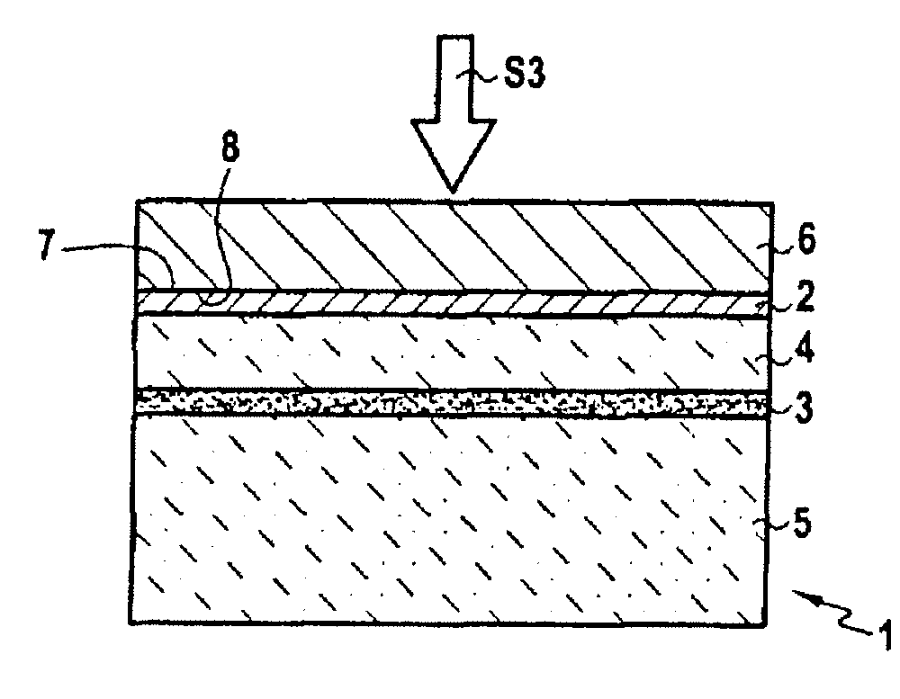
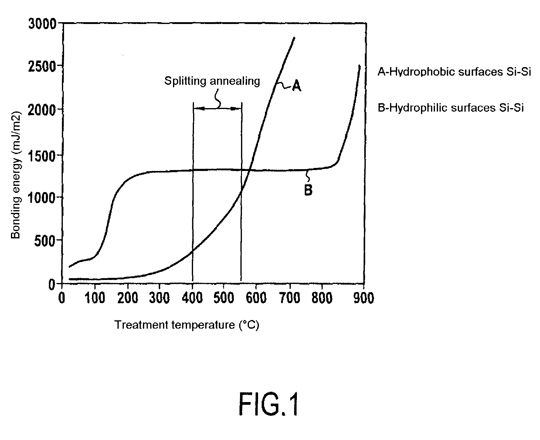
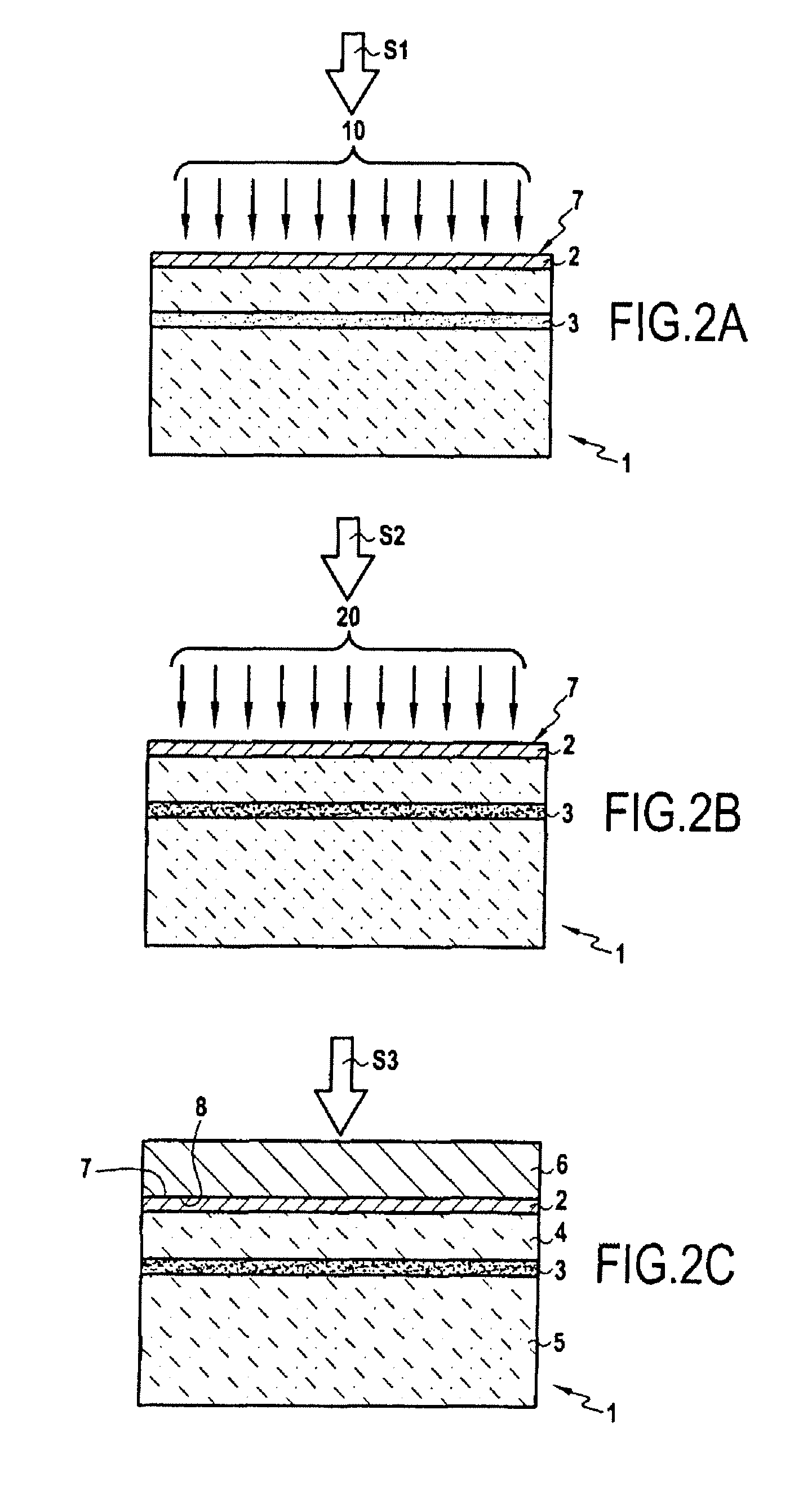
[0037]The present invention applies to any thin layer transfer method using at least one atomic species implantation of a donor substrate to delimit a thin layer to be transferred by a breaking plane, bonding of the implanted donor substrate onto a receiving substrate, and application of a heat treatment called splitting annealing at high temperature to separate the layer to be transferred from the donor substrate as in SMART-CUT® technology.

[0038]The principle of the invention consists of increasing the temperature of splitting annealing required for the formation and development of a weakened zone, comprised of microcavities or platelets, to cause a fracture in the donor substrate so as to increase the bonding energy at the interface between the donor substrate and receiving substrate.

[0039]Typically, splitting annealing in SMART-CUT® technology for substrates of silicon type is conducted over a temperature range of between 400° C. and 500° C. for a determined time (the temperatur...


PUM


Abstract

The invention concerns a method for transferring a thin layer from a donor wafer onto a receiving wafer by implanting at least one atomic species into the donor wafer to form a weakened zone therein, with the weakened zone being including microcavities or platelets therein, and the thin layer being defined between the weakened zone and a surface of the donor wafer; molecular bonding of the surface of the donor wafer onto a surface of the receiving wafer; splitting the thin layer at the zone of weakness by heating to a high temperature to transfer the thin layer to the receiving substrate; and treating the donor wafer to block or limit the formation of microcavities or platelets by trapping the atoms of at least one of the implanted atomic species at least until a certain release temperature is reached during the splitting. This method enables bonding energy to be reinforced adjacent the layer to be transferred and hence limits defects in the resulting heterostructure.

Description

FIELD OF THE INVENTION[0001]The present invention relates to a method for transferring a layer from a donor substrate onto a receiving substrate used for the fabrication of heterostructures such as structures of SeOI type (“Semiconductor on Insulator”) for electronic, microelectronic and optoelectronic applications.BACKGROUND OF THE INVENTION[0002]One well-known technology for producing heterostructures via layer transfer is the SMART-CUT® technology. An example of application of SMART-CUT® technology is described in particular in document U.S. Pat. No. 5,374,564 or in the article by A. J. Auberton-Herve et al titled “Why can Smart-Cut Change the Future of Microelectronics?”, Int. Journal of High Speed Electronics and Systems, Vol. 10, No 1, 2000, p. 131-146. This technology uses the following steps:[0003]a) bombarding the surface of a donor substrate (e.g. in silicon) with light ions of hydrogen or rare gas type (e.g. hydrogen and / or helium), to implant these ions in the substrate ...

Claims


Application Information

Patent Timeline
IPC IPC(8): H01L21/30
CPCH01L21/76254
Inventor HEBRAS, XAVIER
Owner S O I TEC SILICON ON INSULATOR THECHNOLOGIES
Why Eureka
Try Eureka