Method for analyzing characteristic of circuit included in integrated circuit based on process information and the like

Inactive Publication Date: 2008-03-13
PANASONIC CORP
View PDF13 Cites 12 Cited by
  • Summary
  • Abstract
  • Description
  • Claims
  • Application Information

AI Technical Summary

Benefits of technology

[0008]According to the present invention, an influence of variations in an element, such as a device, a wire or the like, included in a semiconductor integrated circuit on a circuit characteristic can be estimated in a short processing time. Even when each device varies at a maximum level, it can be determined whether or not a desired circuit characteristic can be

Problems solved by technology

However, in the conventional statistical delay analyzing technique, a distribution needs to be calculated in the course of calculation of a path delay in a circuit.
Therefore, as compared to the

Method used


Image

  • Method for analyzing characteristic of circuit included in integrated circuit based on process information and the like
  • Method for analyzing characteristic of circuit included in integrated circuit based on process information and the like
  • Method for analyzing characteristic of circuit included in integrated circuit based on process information and the like

Examples


Example

First Embodiment

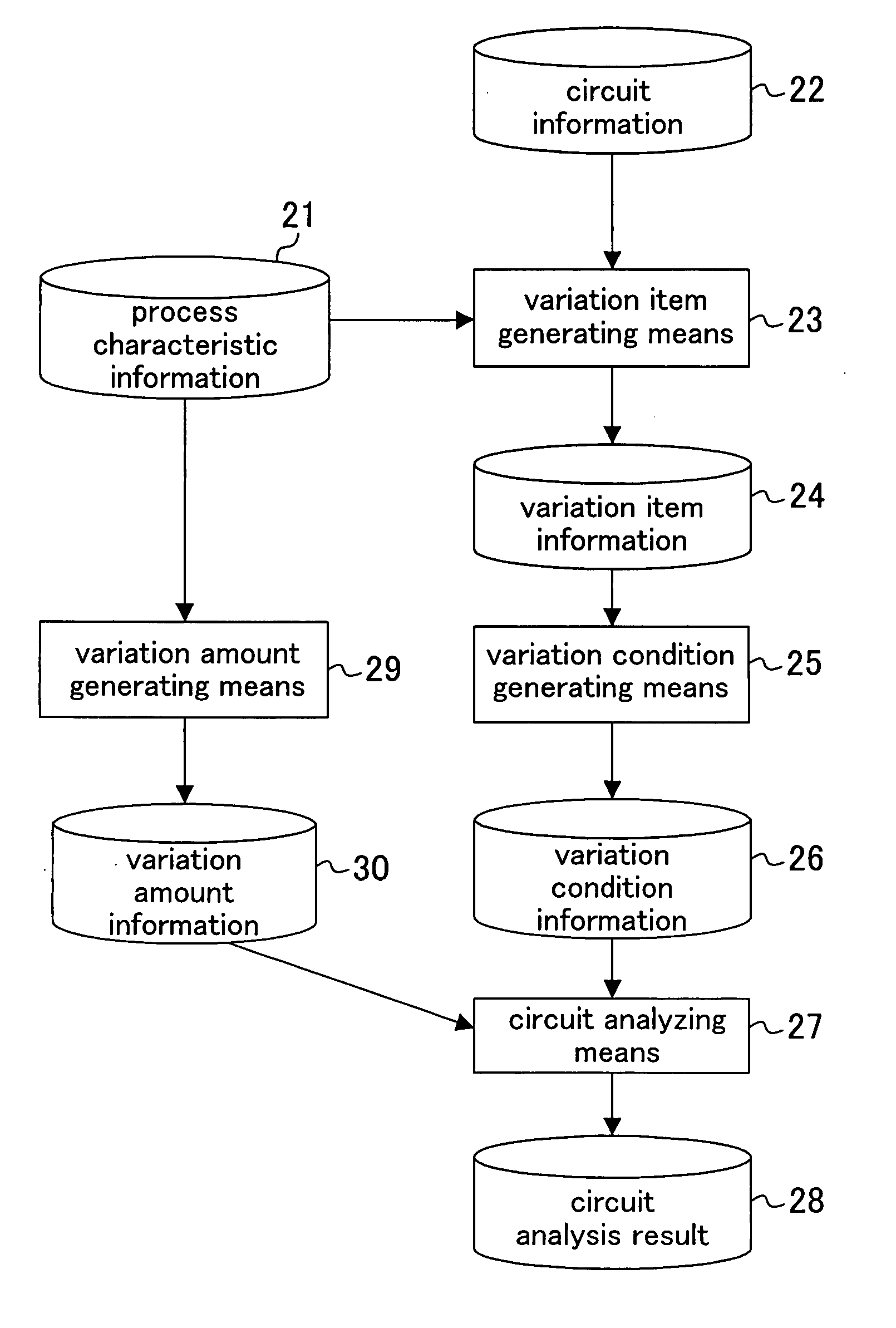
[0082]A flow of a circuit analyzing method according to a first embodiment is shown in FIG. 1. The circuit analyzing method of this embodiment is implemented as a program for causing a computer to execute the flow of FIG. 1 or a device for executing the flow (e.g., a computer for executing the program). Note that the same is true of other embodiments described below.

[0083]

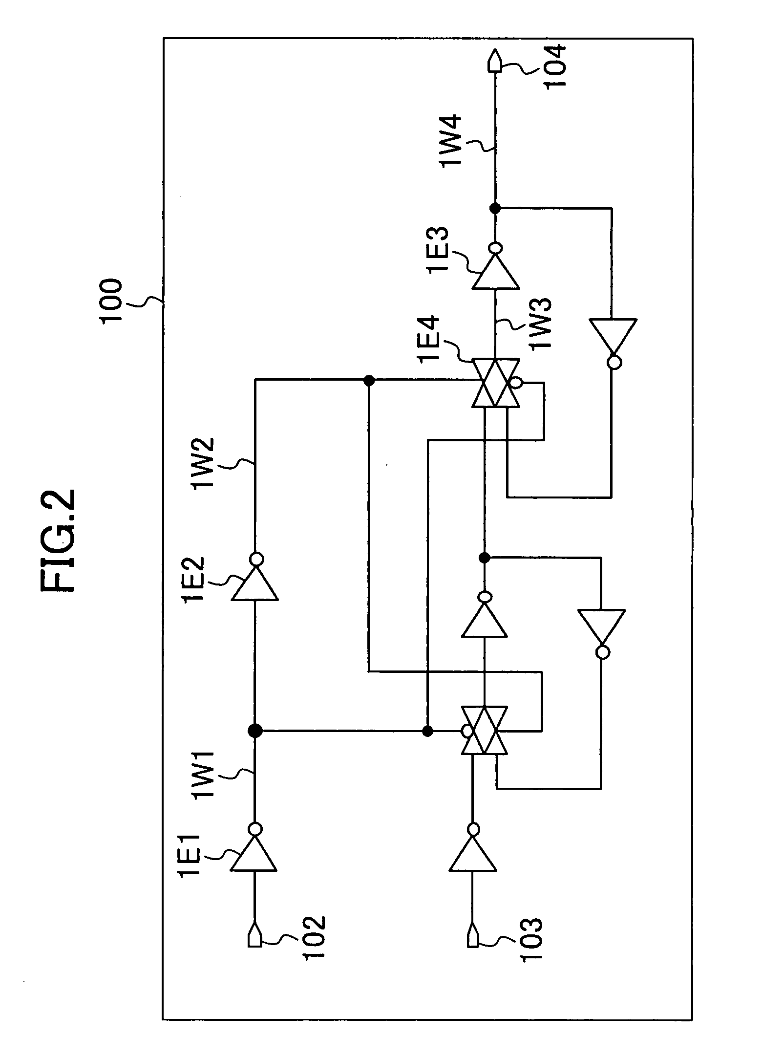
[0084]FIG. 2 shows exemplary circuit information 22 which is to be analyzed by the circuit analyzing method of this embodiment. A method for analyzing a delay in a path from an input terminal 102 to an output terminal 104 (one of the characteristics of a circuit 100) in view of variations in devices 1E1 to 1E4 and wires 1W1 to 1W4 which are elements included in the circuit 100, will be described.

[0085]FIGS. 3 to 5 show exemplary process characteristic information 21. The process characteristic information 21 includes information about the upper limit value, the lower limit value and the like of vari...

Example

Second Embodiment

[0112]

[0113]Next, a second embodiment of the present invention will be described.

[0114]FIG. 14 shows exemplary circuit information 22 which is to be analyzed by a circuit analyzing method of this embodiment. A method for analyzing a characteristic of a circuit 300 in view of variations in devices 3E1 to 3E4 and a capacitance device 3E5 which are included in the circuit 300, will be described. FIG. 15 shows exemplary process characteristic information 21. Maximum and minimum values of variations of change amounts (delvto) of threshold voltages and saturated drain currents (Idsat) of an NMOS (mosn1) and a PMOS (mosp1) are set. A variation width of a capacitance value (value) of a capacitance device (Cap1) is set.

[0115]FIG. 16 shows a flow of a circuit analyzing method according to this embodiment. A variation item grouping means 31 groups a portion of circuit connection relationships and groups variation items based on the circuit information 22 to generate variation ...

Example

Third Embodiment

[0127]

[0128]Transistors paired on a circuit are designed to have similar characteristics, such as the same shape, adjacent positions and the like, and therefore, relative variation amounts (mismatch) in the characteristics between the transistors are small. Therefore, the precision of circuit analysis can be improved by setting the variation amount to be a value which is substantially practical and optimal, depending on a feature of the circuit.

[0129]FIG. 24 is a flowchart of circuit analysis according to this embodiment. A circuit-dependent variation condition generating means 36 extracts a pair of transistors from the circuit information 22 to generate circuit-dependent variation condition information 37. A circuit-dependent variation condition can be generated by a method similar to the above-described variation item grouping means, including, for example, automatic extraction from the circuit information 22 based on the grouping information of FIG. 22 or specific...


PUM


Abstract

A circuit analyzing method of the present invention comprises the steps of (a) applying, for a characteristic having a variation width of characteristics of an element included in a circuit to be analyzed, any one of a maximum value and a minimum value of the variation width as a representative value of the characteristic of the element and (b) estimating a characteristic of the circuit to be analyzed, using the representative value.

Description

CROSS REFERENCE TO RELATED APPLICATIONS[0001]This Non-provisional application claims priority under 35 U.S.C. §119(a) on Patent Application No. 2006-243099 filed in Japan on Sep. 7, 2006, Patent Application No. 2006-305472 filed in Japan on Nov. 10, 2006, and Patent Application No. 2007-165413 filed in Japan on Jun. 22, 2007, the entire contents of which are hereby incorporated by reference.BACKGROUND OF THE INVENTION[0002]1. Field of the Invention[0003]The present invention relates to a technique of simulating a characteristic of a circuit based on process information in design of a semiconductor integrated circuit.[0004]2. Description of the Related Art[0005]In design of semiconductor integrated circuits, advances in miniaturization have led to an increase in influence of process variations on circuit characteristics. Conventionally, variations in delay in each device included in an integrated circuit may be represented by a normal distribution, and a delay distribution in the who...

Claims


Application Information

Patent Timeline
IPC IPC(8): G06F17/50
CPCG06F17/5009G06F17/5081G06F2217/84G06F2217/62G06F2217/10G06F30/398G06F2111/08G06F30/396G06F2119/12G06F30/20
Inventor TANAKA, MASAKAZU
Owner PANASONIC CORP
Why Eureka
Try Eureka