Formulation For Ink-Jet Printing Comprising Semiconducting Polymers

a semi-conducting polymer and inkjet printing technology, applied in the direction of non-metal conductors, sustainable manufacturing/processing, final product manufacturing, etc., can solve the problems of reducing device performance, polymers, like for example the commonly used pat, generally have solubility problems, and lowering electrical performan

Inactive Publication Date: 2008-03-20
MERCK PATENT GMBH
View PDF20 Cites 47 Cited by
  • Summary
  • Abstract
  • Description
  • Claims
  • Application Information

AI Technical Summary

Benefits of technology

[0033] The invention further relates to the use of the formulation as described above and below for the preparation or processing of materials, components or devices that have charge-transport, semiconducting, electrically conducting, photoconducting or light-emitting properties and can be used in optical, electrooptical or electronic components or devices, organic field effect transistors (OFET), integrated circuitry (IC), thin film transistors (TFT), flat panel displays, radio frequency identification (RFID) tags, electroluminescent or photoluminescent devices or components, organic light emitting diodes (OLED), backlights of displays, photovoltaic or sensor devices, charge injection layers, Schottky diodes, planarising layers, antistatic films, conducting substrates or patterns, electrode materials in batteries, photoconductors, electrophotographic applications, electrophotographic recording, organic memory devices, alignment layers, cosmetic or pharmaceutical compositions or for detecting and discriminating DNA sequences.

Problems solved by technology

In addition, it is important that the semiconducting material is relatively stable to oxidation i.e. it has a high ionisation potential, as oxidation leads to reduced device performance.
These polymers, like for example the commonly used PAT, however, do generally have solubility problems for two main reasons.
Introduction of solubilising groups, like for example the alkyl-groups in case of PAT, has the effect of both diluting the electronically active fraction of the material, thus lowering the electrical performance, and may additionally trap charge, depending on the functional groups used.
When this happens in solution, gelling occurs, which, if irreversible, leads to filtration and coating problems.
However, the above documents do not mention the preparation of semiconducting or EL devices by ink-jet printing.
Nor do they provide any technical teaching how to select the solvents and polymers in order to improve the print performance.
The reference further mentions some desired properties of the compositions like viscosity and surface tension, however, the disclosed ranges are very broad and do not provide a technical teaching how to select suitable solvents.
However, there is no technical teaching how to select the solvents and polymers in order to improve the print performance.
However, the formulations described in prior art have several drawbacks.
For example, in case of solutions of polythiophene in chlorinated solvents like chloroform or trichlorobenzene, over time the solvents have been demonstrated to degrade the polythiophene backbone, thus lowering its electrical performance.
In addition, chloroform is too volatile and prematurely evaporates during processing leading to coating irregularities, dispensing problems, loss of resolution and feature definition, as well as clogging of, for example, ink-jet heads.
The solubility of polymers like for example polythiophene in toluene and xylene, on the other hand, is often not high enough to provide sufficient ink viscosity, nor can these solvents achieve a high enough surface tension for reliable ink-jet printing.

Method used


Image

  • Formulation For Ink-Jet Printing Comprising Semiconducting Polymers
  • Formulation For Ink-Jet Printing Comprising Semiconducting Polymers
  • Formulation For Ink-Jet Printing Comprising Semiconducting Polymers

Examples


example 1

[0096] Formulations were prepared from poly(3-hexyl)thiophene (PHT) with a molecular weight of 10,000 and a regioregularity of 96% in different solvents as shown in the table below, and the solubility and gelling behaviour of the polymer were tested.

SurfaceBoilingTensionSolventPoint (° C.)(dynes / cm)Properties of polymerTetralin20734Soluble, heat requiredIndane17635to rapidly dissolve,small amount of gellingover a few days1,2,5-Trichloro-20827Soluble, little gellingbenzeneover time, but remainsa red / brown colourDiethylbenzene18130.5Poor solubility, heatXylene14027.5required and showedvery bad gelling overfew hoursAnisole15432.5Very bad solubilityMethylanisole17431Very bad solubility

[0097] Although anisole and methylanisole have reasonably high boiling points and surface tensions that are higher than the equivalent non-oxygenated aromatic, they showed only a very poor solubilization for the polymer which is insufficient for ink-jet use.

[0098] Xylene and diethylbenzene provided sati...

example 2

[0101] Formulations were prepared from the PHT of example 1 in tetralin and indane at different concentrations as shown in the table below. For comparison a formulation of the PHT in a solvent mixture tetralin / toluene (50 / 50) was prepared.

Formulation No.SolventPHT (wt. %)viscosity (mPa · s)1atetralin1.0%2.531btetralin2.0%3.621cindane1.0%1.722toluene / tetralin1.0%1.28

example 3

Use Example

[0102] The formulations 1a-c and 2 were tested for use as printing inks.

[0103] A) To test the priming performance the inks were loaded into a Spectra SX-128 ink-jet printhead (available from Spectra Inc., NH, USA). The head reservoir was half filled with ink (about 10 ml); ink was primed through the nozzles using a single purge at a pressure of 5.5 PSI for 5 seconds (a standard purge on the Spectra Apollo system).

[0104] B) To investigate jetting properties and droplet formation under different driving conditions, the formulations were loaded into the

[0105] Spectra SX Special print head and then jetted using a variety of firing voltages, frequencies and waveforms.

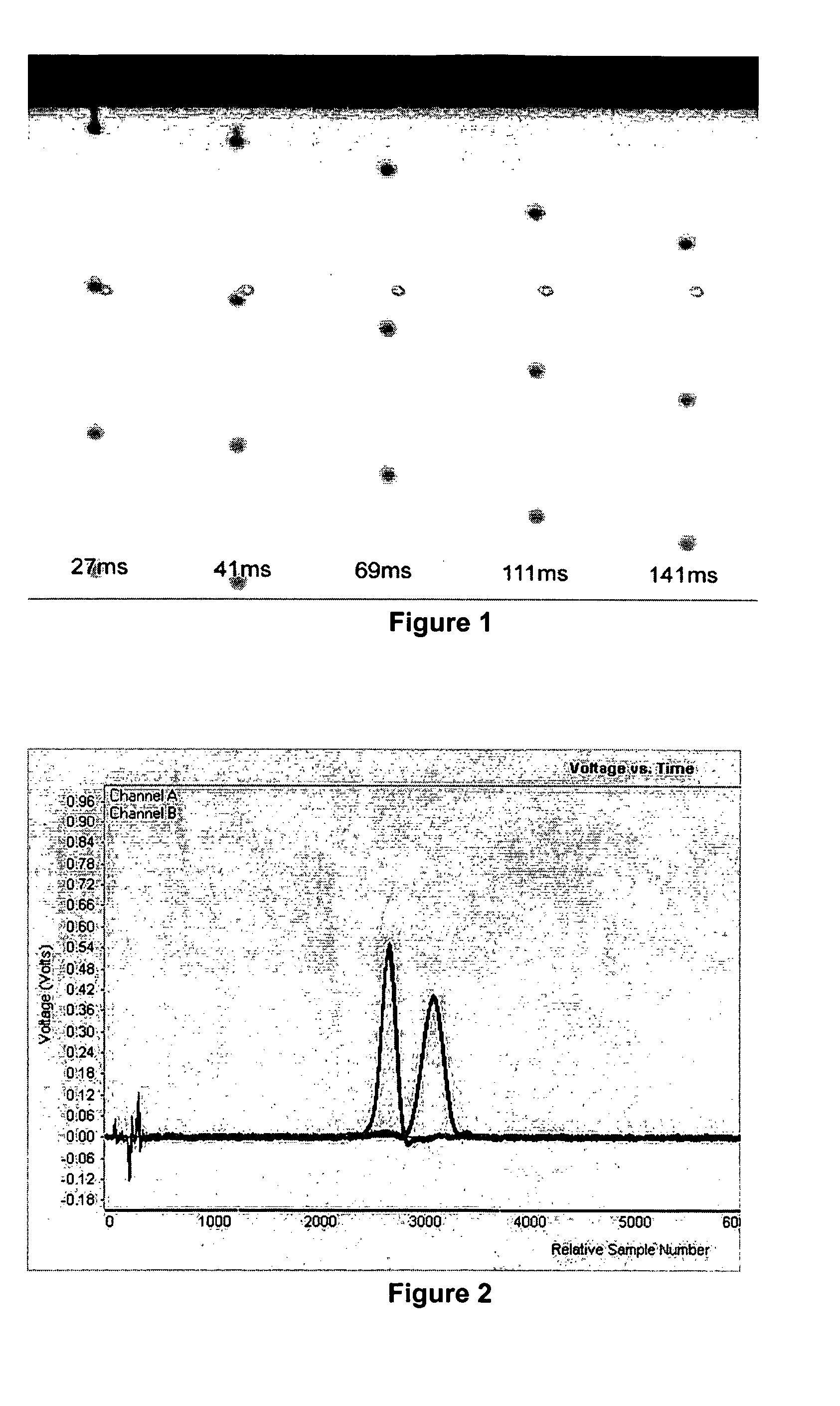
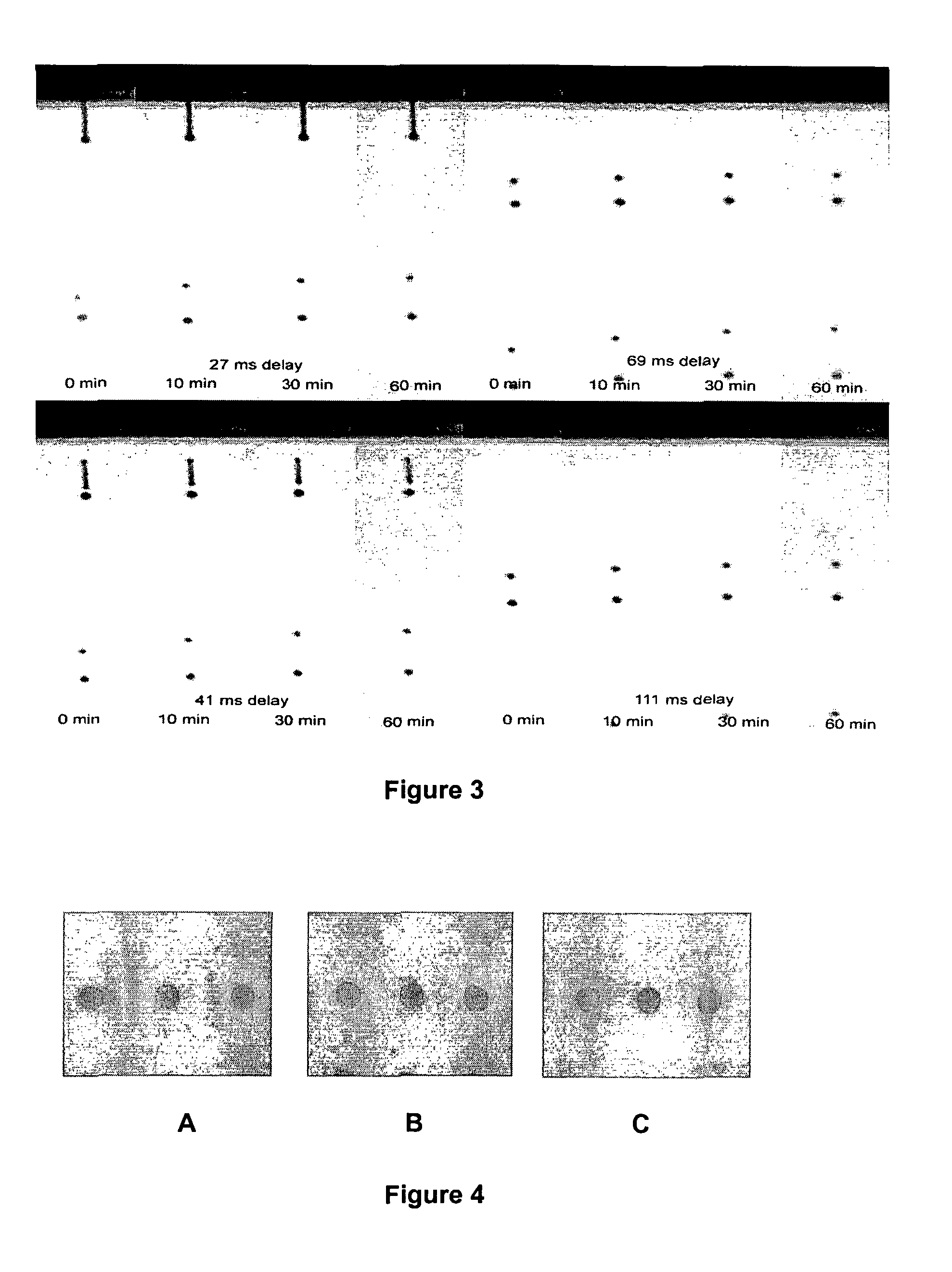
[0106] C) To investigate the dwell performance of the inks the head was first primed and drops were jetted—images of these were recorded. The head was then left for a set length of time, either 5 or 30 minutes without firing. After this time the head was fired and images immediately recorded at different dela...


PUM

PropertyMeasurementUnit
boiling temperatureaaaaaaaaaa
surface tensionaaaaaaaaaa
viscosityaaaaaaaaaa

Abstract

The invention relates to formulations comprising one or more polymers with semiconducting, charge transport, photoconducting and/or photo- or electroluminescent properties and one or more organic solvents, to their use for the preparation of electrooptical or electronic devices, including field effect transistors (FETs), electroluminescent, photovoltaic and sensor devices, in particular by ink-jet printing, and to FETs and other semiconducting or light emitting components or devices comprising the formulations.

Description

FIELD OF INVENTION [0001] The invention relates to formulations comprising one or more polymers with semiconducting, charge transport, photoconducting and / or photo- or electroluminescent properties and one or more organic solvents. The invention further relates to the use of the formulations for the preparation of electrooptical or electronic devices, including field effect transistors (FETs), electroluminescent, photovoltaic and sensor devices, in particular by ink-jet printing. The invention further relates to FETs and other semiconducting or light-emitting components or devices comprising the formulations. BACKGROUND AND PRIOR ART [0002] Organic materials with semiconducting or charge-transport properties have recently shown promise as the active layer in organic based thin film transistors (TFT) and organic field effect transistors (OFETs) [see H. E. Katz, Z. Bao and S. L. Gilat, Acc. Chem. Res., 2001, 34, 5, 359]. Such devices have potential applications in smart cards, securit...

Claims


Application Information

Patent Timeline
Patent Type & Authority Applications(United States)
IPC IPC(8): H01L51/40H01L51/00H01L51/05H01L51/30
CPCH01L51/0005H01L51/0007Y02E10/549H01L51/0512H01L51/0036Y02P70/50H10K71/15H10K71/135H10K85/113H10K10/462C09D11/30C08L101/12H10K10/00
Inventor MCCULLOCH, IAINSPARROWE, DAVIDSHKUNOV, MAXIMBENTLEY, PHILGILES, MARK
Owner MERCK PATENT GMBH
Why Eureka
Try Eureka