Avalanche photodiode

a photodiode and photodiode technology, applied in the field of photodiodes, can solve the problems of reducing the signal-to-noise ratio of the detector, high random multiplication, and considerable noise factor, and achieve the effect of accelerating the photocarriers towards the p-n junction even faster and reducing the detector's response tim

Active Publication Date: 2008-03-20
COMMISSARIAT A LENERGIE ATOMIQUE ET AUX ENERGIES ALTERNATIVES
View PDF5 Cites 23 Cited by
  • Summary
  • Abstract
  • Description
  • Claims
  • Application Information

AI Technical Summary

Benefits of technology

[0053]Such a metallisation layer makes it possible, by applying an appropriate bias voltage, to accumulate charge carriers at the interface between the semiconductor materials and the passivation layer which is inherently neutral, i.e. on the flanks of the “mesas”. The charge carriers thus accumulated form an electric field capable of accelerating the photocarriers towards the p-n junction even faster, and this helps reduce the detector's response time.

Problems solved by technology

However, in most avalanche diodes according to the prior art, such amplification of small currents causes amplification of electronic noise and hence degrades the detector's signal-to-noise ratio.
In particular, if impact ionisation is produced by holes and electrons, multiplication is highly random and the noise factor is considerable (F>2).
In a known manner, the dark current contributes to degradation of the detector's signal-to-noise ratio for the smallest stream of photons that is to be measured, thus limiting the sensitivity of the detector for a given bias.
This dark current limits the sensitivity of the detector.
Consequently, sensitivity deteriorates when the detector is operating at high temperature.

Method used


Image

  • Avalanche photodiode
  • Avalanche photodiode
  • Avalanche photodiode

Examples


Embodiment Construction

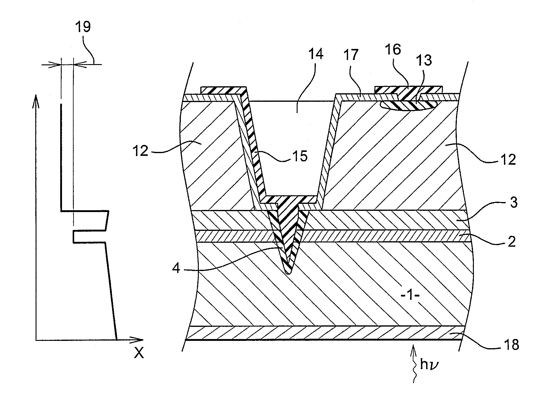
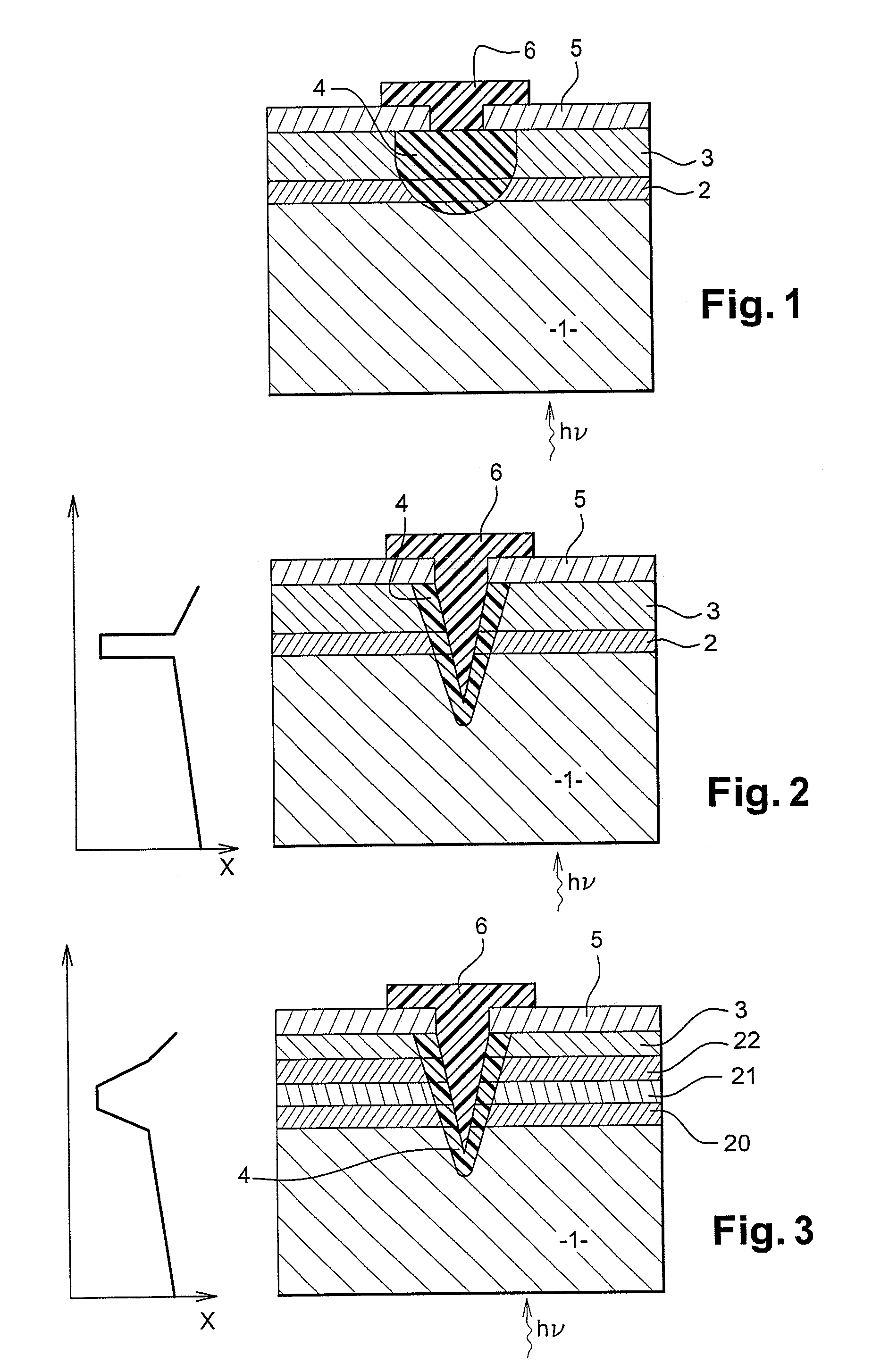
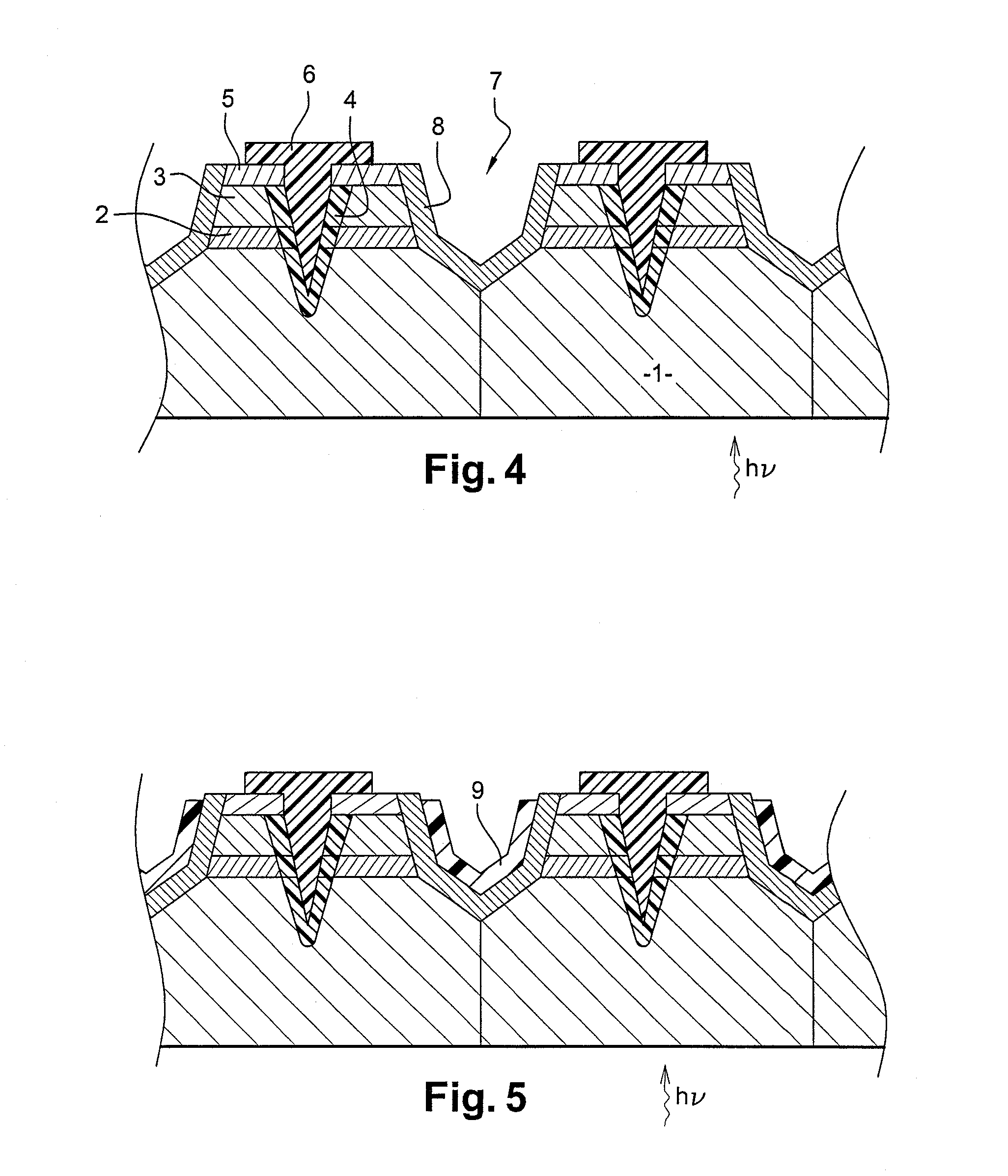
[0064]FIG. 1 therefore shows a diode according to a first embodiment of the invention in which interaction layer 1 is designed to interact with incident photons of electromagnetic radiation such as infrared rays or visible light rays. Interaction layer 1 therefore preferably extends transversely or even at right angles to the direction of the incident photons that are to be detected.

[0065]In practice, layer 1 consists of a semiconductor material with a first conductivity type, for example an alloy of mercury, cadmium and tellurium having the formula Hg1-xCdxTe. The thickness of the interaction layer, i.e. the height dimension in FIGS. 1 to 6, is selected depending on the wavelength of the radiation to be detected.

[0066]Thus, when short-wavelength infrared rays (λ6 μm) are to be detected, the thickness of interaction layer 1 may exceed 1 μm, 3 μm or 6 μm respectively.

[0067]Conventional deposition techniques are used to cover interaction layer 1 with collection layer 2 designed to col...


PUM


Abstract

A photodiode designed to capture incident photons includes a stack of at least three superposed layers of semiconductor materials having a first conductivity type The stack includes: an interaction layer designed to interact with incident photons so as to generate photocarriers, a collection layer to collect the photocarriers; a confinement layer designed to confine the photocarriers in the collection layer. The collection layer has a band gap less than the band gaps of the interaction layer and confinement layer. The photodiode also includes a region which extends transversely relative to the planes of the layers. The region is in contact with the collection layer and confinement layer and has a conductivity type opposite to the first conductivity type so as to form a p-n junction with the stack.

Description

FIELD OF THE INVENTION[0001]The present invention relates to a photodiode intended, by definition, to capture photons, especially when it functions in the reverse bias avalanche operating mode.[0002]The present invention also relates to a detector comprising juxtaposed photodiodes of this type.[0003]The present invention therefore relates to the field of optoelectronic components and detectors.DESCRIPTION OF THE PRIOR ART[0004]In a known manner, avalanche diodes are used in order to detect streams of incoming photons in a relatively sensitive and / or relatively fast manner, i.e. with short response times. In fact, an avalanche photodiode allows detection with amplification of photocarriers when the reverse bias is sufficient to trigger avalanche behaviour in the multiplication region.[0005]Thus, avalanche photodiodes have various possible applications including implementing detection focal-planes for active imaging, high-speed detection in the field of telecommunications, spectroscop...

Claims


Application Information

Patent Timeline
Patent Type & Authority Applications(United States)
IPC IPC(8): H01L31/107
CPCH01L31/03529Y02E10/50H01L31/107
Inventor ROTHMAN, JOHAN
Owner COMMISSARIAT A LENERGIE ATOMIQUE ET AUX ENERGIES ALTERNATIVES
Why Eureka
Try Eureka