

Multi-layer ceramic capacitor
a multi-layer ceramic and capacitor technology, applied in the direction of fixed capacitors, stacked capacitors, fixed capacitor details, etc., can solve the problems of large capacitance multi-layer ceramic capacitors and difficult to obtain small sizes
- Summary
- Abstract
- Description
- Claims
- Application Information
AI Technical Summary
Benefits of technology
Problems solved by technology
Method used
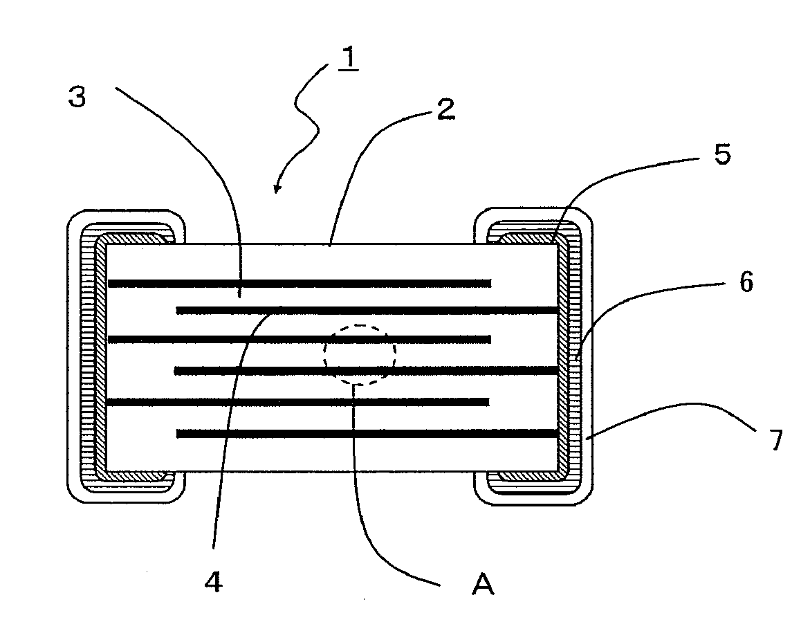
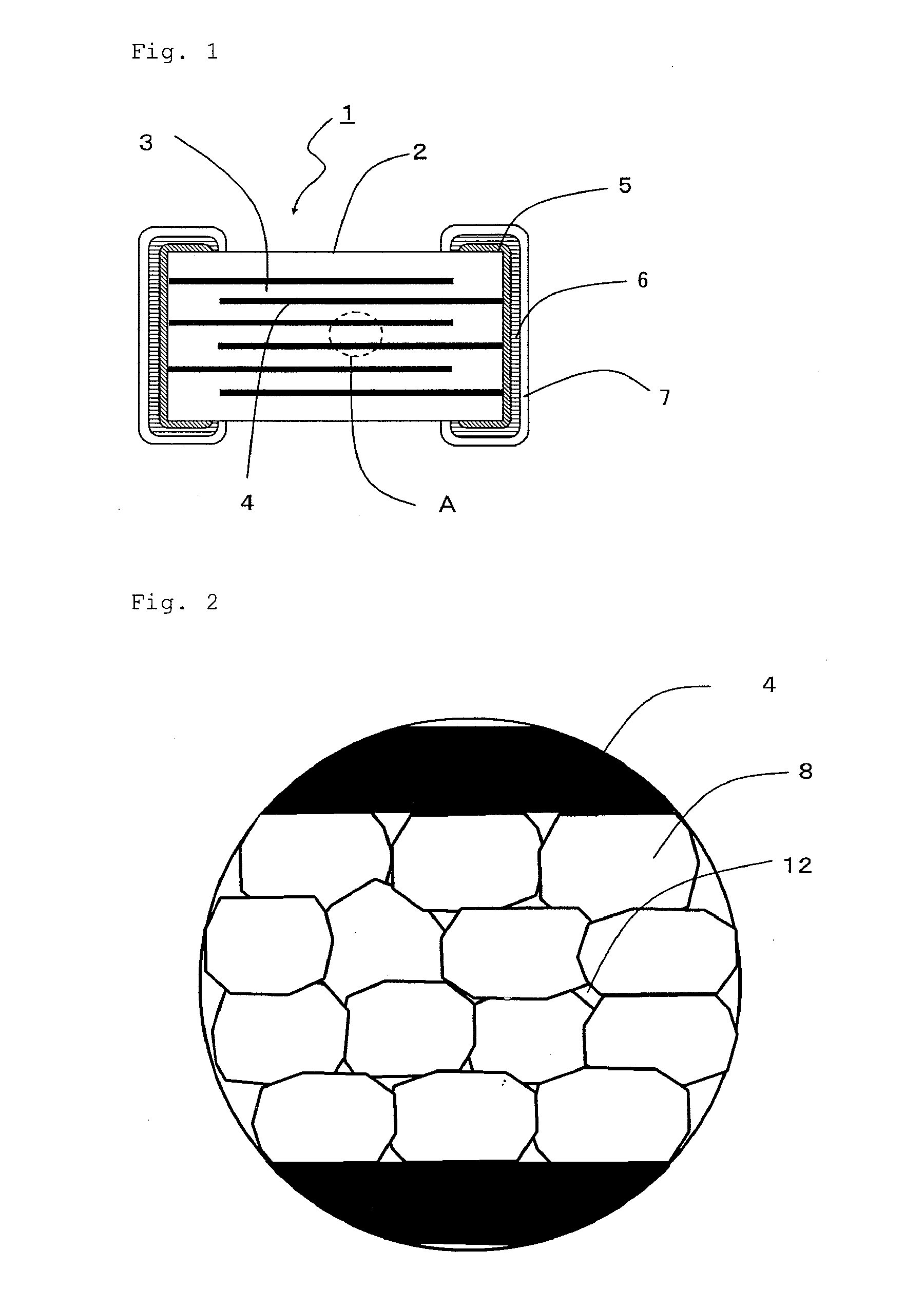
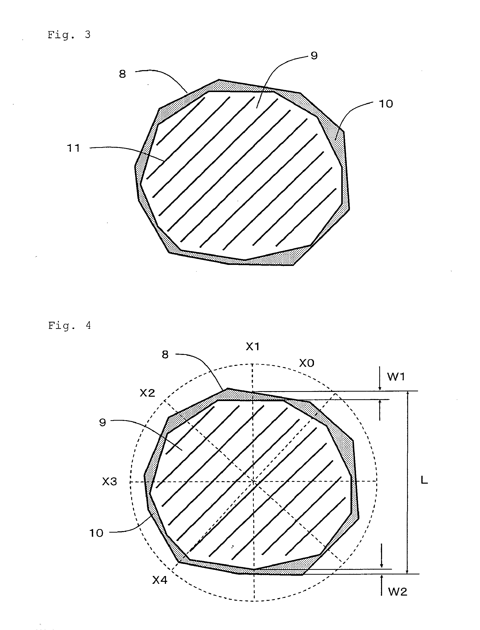
Image

Examples
example 1
[0034]A starting material M3 in table 1 was provided, which was wet-mixed for 15 hours in a ball mill, calcined at 400° C. for 2 hours in an atmospheric air after drying and dry-pulverized to obtain a dielectric material powder. Then, polyvinyl butylal, an organic solvent, and a plasticizer were admixed to the powder to form a ceramic slurry. The ceramic slurry was sheeted by a roll coater to obtain a ceramic green sheet of 5 μm thickness. A Cu internal electrode paste (specimen 1-1) or an Ni internal electrode paste (specimen 1-2) was coated on the ceramic green sheet by screen printing to form an internal electrode pattern. Ceramic green sheets on which the internal electrode pattern was formed were stacked by the number of 20 sheets, press bonded, and then cut and divided each into a size of 4.0×2.0 mm to form green chips. The green chip was removed with the binder in a nitrogen atmosphere and, successively, baked at a baking temperature shown in Table 2 in a reducing atmosphere....
example 2
[0037]A starting material M4 in Table 1 was provided and multi-layer ceramic capacitors were formed in the same manner as in Example 1 except for using the conditions of the stirring time for the wet mixing and the baking temperature shown in Table 3. The average value for the grain size, t / D, the permittivity, the temperature characteristic, and the high temperature acceleration life time were measured and collectively shown in Table 3.
TABLE 3DielectricStirringBakingGraincharacteristicSpecimenDielectrictimeInternaltemperaturesizeTemperatureLife timeNo.material(hr)Electrode(° C.)(μm)t / DPermittivitycharacteristiccharacteristic2-1M415Cu10000.334%2520X8R◯2-2M420Cu10000.335%2540X8R◯2-3M425Cu10000.357%2680X7R◯2-4M430Cu10000.3510%2700X7R◯2-5M440Cu10000.3515%2750NG◯2-6M415Cu9800.332%2480X8R◯2-7M415Cu9600.331%2420X8RX
[0038]From the results described above, those specimens using the internal electrodes formed of Cu, having the average value for the diameter of the grains of 400 nm or less an...
example 3
[0039]Starting materials M1 and M2 in Table 1 were provided, multi-layer ceramic capacitors were formed in the same manner as in Example 1, and the average value for the grain size, t / D, the permittivity, the temperature characteristic, and the high temperature acceleration life time were measured and collectively shown in Table 4. In this case, the effect of the additives was verified.
TABLE 4DielectricStirringBakingGraincharacteristicSpecimenDielectrictimeInternaltemperaturesizeTemperatureLife timeNo.material(hr)Electrode(° C.)(μm)t / DPermittivitycharacteristiccharacteristic3-1M115Cu10000.304%2050X8RX3-2M215Cu10000.367%2810X7RX
[0040]From the results described above, it was found that the life time property was lowered in a case where only one of the Mn oxides and the rare earth oxides was contained as the additives.
PUM
| Property | Measurement | Unit |
|---|---|---|
| Temperature | aaaaa | aaaaa |
| Fraction | aaaaa | aaaaa |
| Fraction | aaaaa | aaaaa |
Abstract
Description
Claims
Application Information