Methods for forming an organic thin film using solvent effects, organic thin film formed by the method, and organic electronic device comprising organic thin film

Inactive Publication Date: 2008-03-20
SAMSUNG ELECTRONICS CO LTD
View PDF5 Cites 3 Cited by
  • Summary
  • Abstract
  • Description
  • Claims
  • Application Information

AI Technical Summary

Benefits of technology

[0011]Example embodiments have been made to meet the technical need in the art, and example embodiments provide a novel method for forming an organic thin film using solvent effects in an easy manner by a simple wet process in which a good solvent and a non-solvent may be used to induce aggregation of an organic material in a solution and subsequently to promote crystallization of the organic material by virtue of the aggregation, thereby achieving improved physical properties and improved surface characteristics of the organic thin film. Example embodiments provide an inexpensive organic electronic device with improved electrical properties which may include a thin film formed by the method.

Problems solved by technology

Vacuum evaporation has the problem of a complicated and troublesome procedure and may be thus inefficient in terms of processing.
Because vacuum evaporation requires an increased temperature of about 200° C. to about 400° C. to form thin films, various substrates may be limited in their use and printing processes may be difficult to apply to the fabrication of devices using the thin films.
The performance of organic thin films formed by room-temperature wet processes may not reach that of organic thin films formed by vacuum evaporation.
These approaches have a limitation in improving the characteristics of thin films in that complicated additional steps may be required and the treatments may be done in a state where the degree of freedom of materials for thin films is limited.

Method used


Image

  • Methods for forming an organic thin film using solvent effects, organic thin film formed by the method, and organic electronic device comprising organic thin film
  • Methods for forming an organic thin film using solvent effects, organic thin film formed by the method, and organic electronic device comprising organic thin film
  • Methods for forming an organic thin film using solvent effects, organic thin film formed by the method, and organic electronic device comprising organic thin film

Examples


example 1

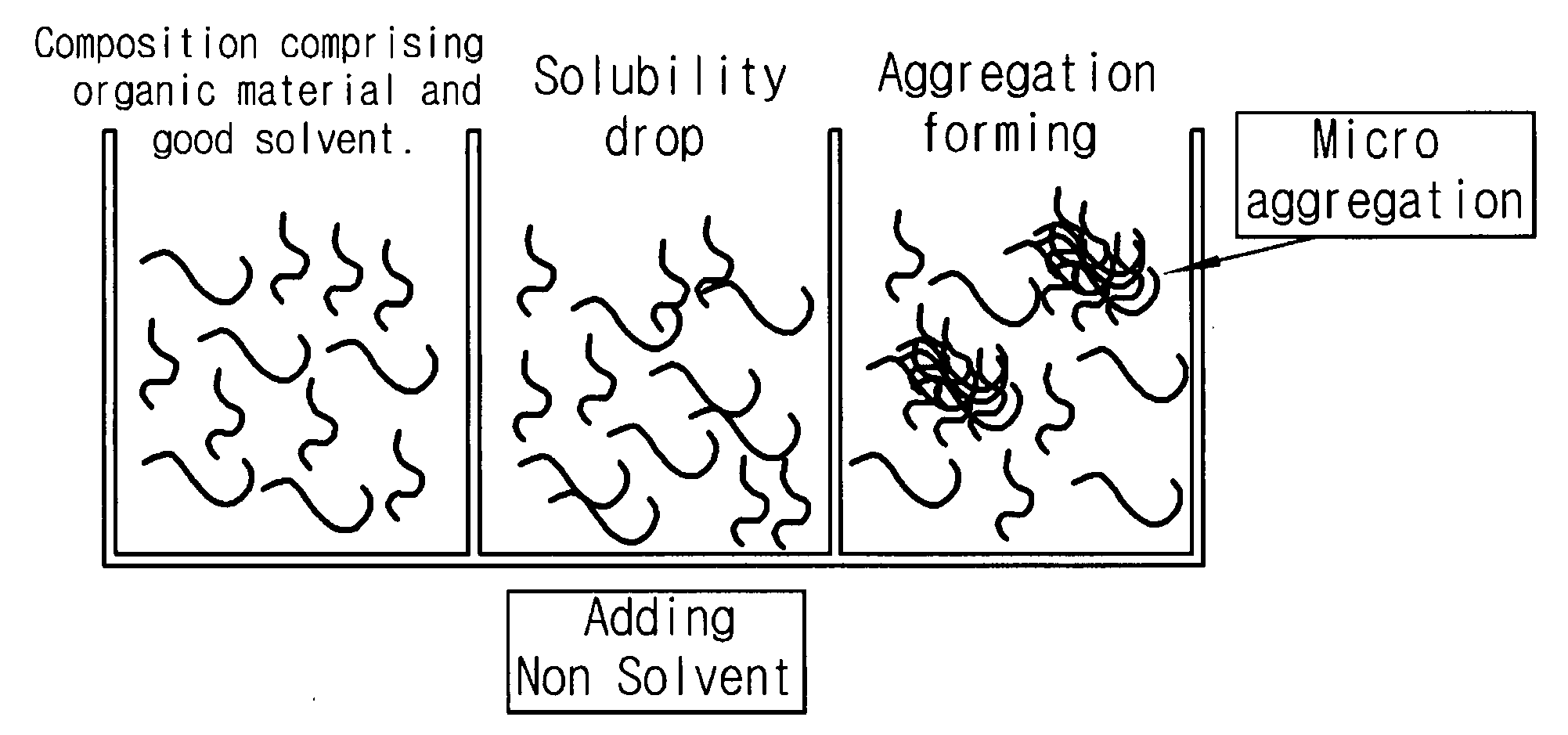
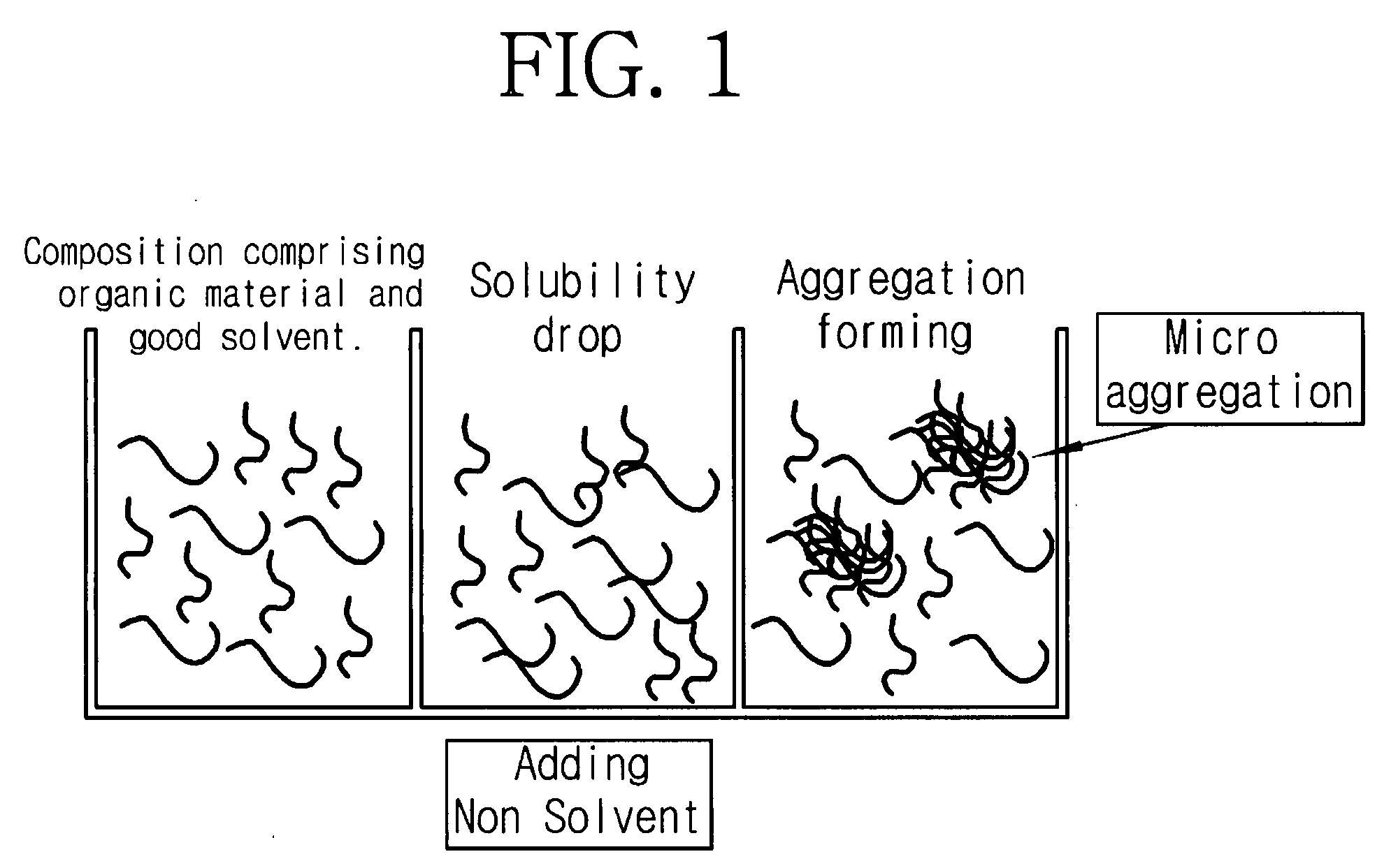
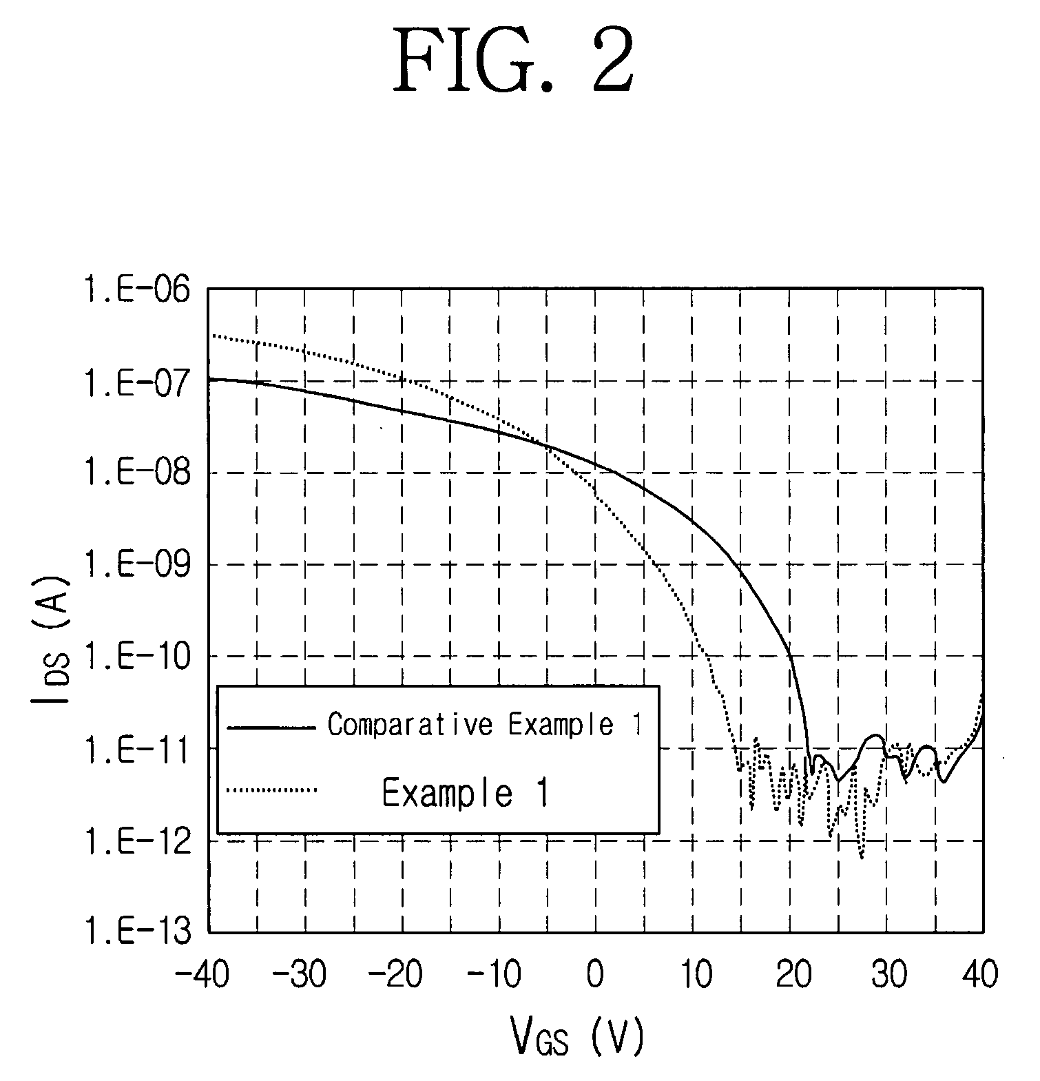
[0066]About 1 wt % of poly(3-hexylthiophene) (P3HT) (molecular weight: about 33,000) was dissolved in chlorobenzene at about 45° C., and then about 10 parts by volume of acetonitrile was added to the solution. The mixture was dispersed by sonication for about 3 hours to prepare an organic semiconductor composition. A molybdenum / tungsten (Mo / W) alloy was deposited to a thickness of about 1,000 Å on a clean glass substrate by sputtering to form a gate electrode. Then a mixture of the methacryloxypropyltrimethoxysilane polymer and tetrabutoxy titanate (Ti(OC4H9)4)(about 70:30 weight ratio) was dissolved in butanol a concentration of about 10 wt %. The solution was spin-coated to a thickness of about 7,000 Å thereon to form a gate insulating layer. The organic semiconductor composition was spin-cast at about 1,000 rpm to a thickness of about 800 Å on the gate insulating layer, and baked under a nitrogen atmosphere at about 100° C. for about 10 minutes to form a semiconductor layer. Ther...

example 2

[0067]About 1 wt % of poly(3-hexylthiophene) (P3HT) (molecular weight: about 33,000) was dissolved in chlorobenzene at about 45° C., and then about 10 parts by volume of butyl alcohol was added to the solution. The mixture was dispersed by sonication for about 3 hours to prepare an organic semiconductor composition. A molybdenum / tungsten (Mo / W) alloy was deposited to a thickness of about 1,000 Å on a clean glass substrate by sputtering to form a gate electrode, and then an organic insulator material was spin-coated to a thickness of about 7,000 Å thereon to form a gate insulating layer. As the organic insulator material, the same material as that used in Example 1 was used. The organic semiconductor composition was spin-cast at about 1,000 rpm to a thickness of about 800 Å on the gate insulating layer, and baked under a nitrogen atmosphere at about 100° C. for about 10 minutes to form a semiconductor layer. Thereafter, gold (Au) was deposited to a thickness of about 700 Å on the sem...

example 3

[0068]About 1 wt % of poly(3-hexylthiophene) (P3HT) (molecular weight: about 33,000) was dissolved in chlorobenzene at about 45° C. and dispersed by sonication for about 3 hours to prepare an organic semiconductor composition. A molybdenum / tungsten (Mo / W) alloy was deposited to a thickness of about 1,000 Å on a clean glass substrate by sputtering to form a gate electrode, and then an organic insulator material was spin-coated to a thickness of about 7,000 Å thereon to form a gate insulating layer. As the organic insulator material, the same material as that used in Example 1 was used. A predetermined or given amount of the organic semiconductor composition was drop-cast on the gate insulating layer. Before evaporation of the solvent, butyl alcohol was dropped on the organic semiconductor composition. The butyl alcohol was used in an amount of about 10% by volume, based on the volume of the composition. The resulting structure was baked under a nitrogen atmosphere at about 100° C. fo...


PUM


Abstract

Disclosed is a method for forming an organic thin film using a good solvent and a non-solvent to promote crystallization of an organic material. The method may enable the formation of a dense, uniform, highly ordered organic thin film by a wet process in a simple and an economical manner. Therefore, the organic thin film may be used as a gate insulating layer or a semiconductor layer to fabricate an organic electronic device having improved electrical properties, e.g., increased charge carrier mobility. Further disclosed are an organic thin film formed by the method and an organic electronic device including the organic thin film.

Description

PRIORITY STATEMENT[0001]This non-provisional application claims priority under 35 U.S.C. § 119 to Korean Patent Application No. 2006-0090109, filed on Sep. 18, 2006, in the Korean Intellectual Property Office (KIPO), the entire contents of which are herein incorporated by reference.BACKGROUND[0002]1. Field[0003]Example embodiments relate to a method for forming an organic thin film using solvent effects and its applications. Other example embodiments relate to a method for forming an organic thin film in which a good solvent and a non-solvent may be used to promote crystallization of an organic material, an organic thin film formed by the method, and an organic electronic device including the organic thin film.[0004]2. Description of the Related Art[0005]Generally, the characteristics of organic electronic devices may be determined by various factors, e.g., density, uniformity, cleanness, adhesiveness and ordering degree, of organic thin films for use in the organic electronic devic...

Claims


Application Information

Patent Timeline
IPC IPC(8): H01L51/00
CPCH01L51/0007Y02E10/549H01L51/0558H01L51/0026H10K71/15H10K71/40H10K10/484
Inventor HAHN, JUNG SEOKLEE, BANG-LINKIM, TAE-SANGLEE, SANG-YOONMOON, HYUN SIK
Owner SAMSUNG ELECTRONICS CO LTD
Why Eureka
Try Eureka