Aspect ratio trapping for mixed signal applications

a technology of mixed signal and aspect ratio, applied in the field of semiconductor processing, can solve the problems of inability to connect si and iii-v devices, inability to accept dislocation defect levels, and inability to meet the requirements of cmos front- and back-end processing restrictions,

Inactive Publication Date: 2008-03-20
AMBERWAVE SYST
View PDF99 Cites 187 Cited by
  • Summary
  • Abstract
  • Description
  • Claims
  • Application Information

AI Technical Summary

Benefits of technology

[0005] Selective epitaxy is suitable for the integration of heterogeneous compound semiconductors on substrates incorporating lattice-mismatched materials, such as Si, due to its flexibility and relative simplicity in comparison to oth...

Problems solved by technology

Growing such films directly on Si may lead to unacceptable dislocation defect levels.
Taking GaAs as an example, growing more than a few nanometers (nm) directly on Si typically leads to a dislocation density of 108-109/cm2 due to the lattice mismatch between the two materials.
Requiring such vertical displacement between the Si and III-V devices is generally incompatible with Si CMOS technology, and may make interconnection betwee...

Method used


Image

  • Aspect ratio trapping for mixed signal applications
  • Aspect ratio trapping for mixed signal applications
  • Aspect ratio trapping for mixed signal applications

Examples


Embodiment Construction

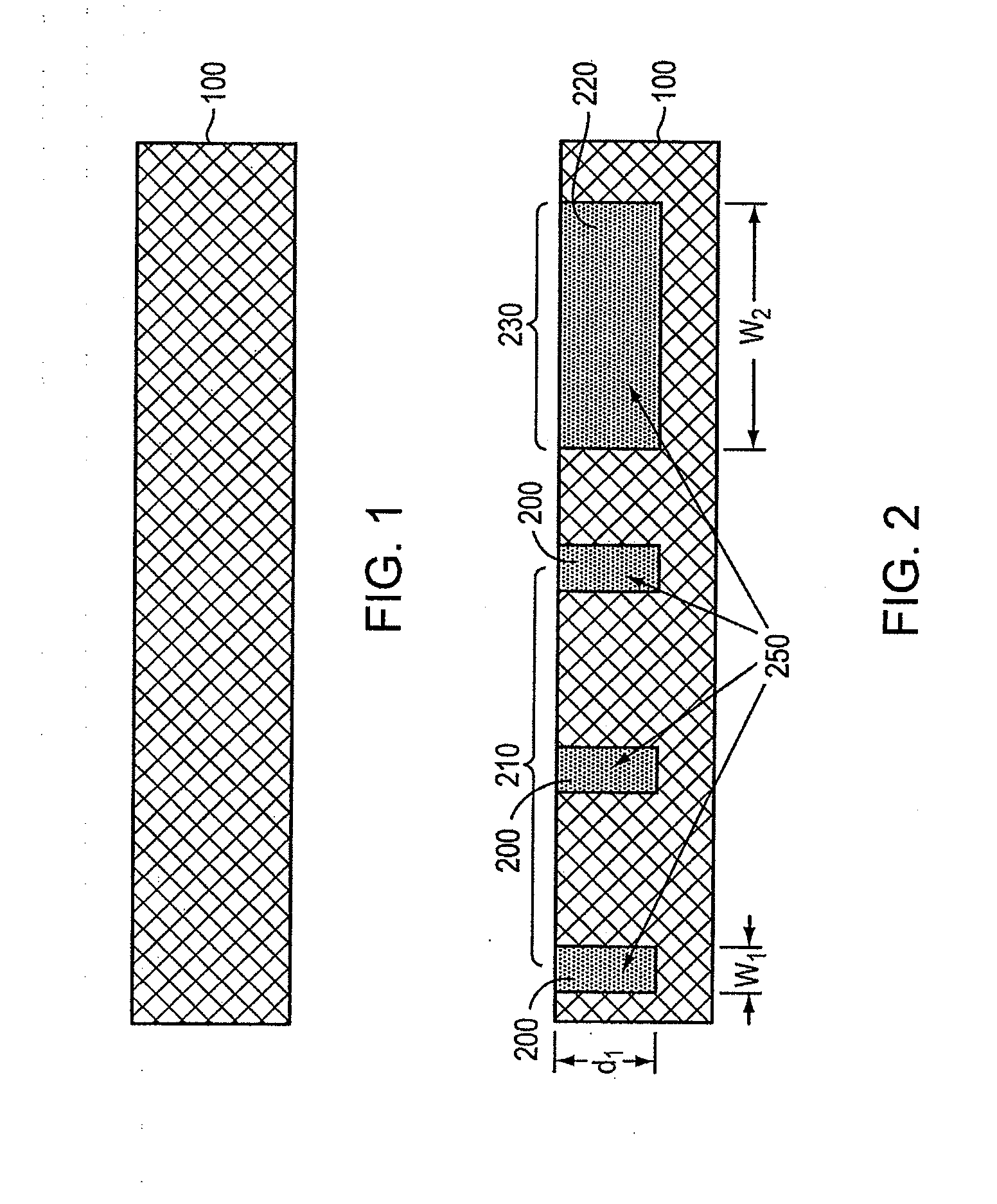
[0034] Referring to FIG. 1, a substrate 100 includes a crystalline semiconductor material. The substrate 100 may be, for example, a bulk silicon wafer, a bulk germanium wafer, a semiconductor-on-insulator (SOI) substrate, or a strained semiconductor-on-insulator (SSOI) substrate. The substrate 100 may include or consist essentially of a first semiconductor material, such as a group IV element, e.g., germanium or silicon. In an embodiment, substrate 100 includes or consists essentially of (100) silicon.

[0035] ART is used to create a relatively defect-free portion of an epitaxial region disposed in an opening over the substrate. As used herein, ART refers generally to the technique(s) of causing defects to terminate at non-crystalline, e.g., dielectric sidewalls, where the sidewalls are sufficiently high relative to the size of the growth area so as to trap most, if not all, of the defects. This technology allows the growth of an epitaxial material directly in contact with a lattice-...


PUM


Abstract

Structures and methods for their formation include a substrate comprising a first semiconductor material, with a second semiconductor material disposed thereover, the first semiconductor material being lattice mismatched to the second semiconductor material. Defects are reduced by using an aspect ratio trapping approach.

Description

RELATED APPLICATIONS [0001] This application claims the benefit of and priority to U.S. Provisional Application Ser. No. 60 / 845,303 filed Sep. 18, 2006, the disclosure of which is hereby incorporated by reference in its entirety.FIELD OF THE INVENTION [0002] This invention relates generally to semiconductor processing and particularly to integration of mixed digital and analog devices. BACKGROUND OF THE INVENTION [0003] Many (if not most) modern electronic devices incorporate both digital circuits and analog circuits. Devices such as cellular telephones, digital TV receivers, and computers perform both information processing and storage functions as well as communication functions. In these devices, the information processing and storage is performed primarily by digital circuits while the communication functions are accomplished using mostly analog circuits. [0004] Historically, semiconductor technologies designed for digital functions have evolved separately from semiconductor tec...

Claims


Application Information

Patent Timeline
IPC IPC(8): H01L21/338
CPCH01L21/02381H01L21/02538H01L27/0605H01L21/823412H01L21/8258H01L21/02551
Inventor LOCHTEFELD, ANTHONY J.FIORENZA, JAMES
Owner AMBERWAVE SYST
Why Eureka
Try Eureka