Polishing Apparatus

a technology of polishing apparatus and rotary blade, which is applied in the direction of grinding drive, lapping machine, manufacturing tools, etc., can solve the problems of short circuit, large step height on the surface of the semiconductor device, and complicated structure of the semiconductor elemen

Active Publication Date: 2008-03-20
EBARA CORP
View PDF30 Cites 62 Cited by
  • Summary
  • Abstract
  • Description
  • Claims
  • Application Information

AI Technical Summary

Benefits of technology

[0012] The present invention has been made in view of the above drawbacks. It is, therefore, a first object of the present invention to provide a polishing apparatus which can polish a substrate ...

Problems solved by technology

In recent years, semiconductor devices have become more integrated, and structures of semiconductor elements have become more complicated.
Accordingly, irregularities on a surface of a semiconductor device are increased, so that step heights on the surface of the semiconductor device tend to be large.
When the number of irregularities is increased on a surface of a semiconductor device, the following problems arise.
Further, an open circuit may be caused by disconnection, or a short circuit may be caused by insufficient insulation between interconnection layers.
As a result, good products cannot be obtained, and the yield tends to be lowered.
Further, even if a semiconductor device initially works normally, reliability of the semiconductor device is lowered after a long-term use.
Therefore, if the irregularities on the surface of the semiconductor device are increased, then it becomes problematically difficult to form a fine pattern itself on the semiconductor device.
In such a polishing apparatus, the polishing pad is so elastic that pressing forces app...

Method used


Image

  • Polishing Apparatus
  • Polishing Apparatus
  • Polishing Apparatus

Examples


first embodiment

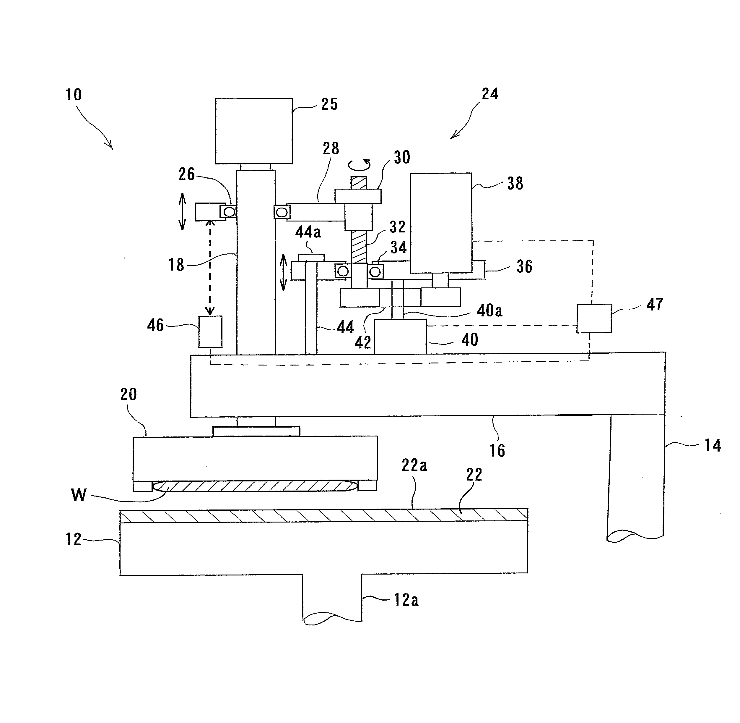
[0074]FIG. 1 is a schematic view showing a polishing apparatus 10 according to the present invention. As shown in FIG. 1, the polishing apparatus 10 has a polishing table 12, a top ring head 16 connected to an upper end of a support shaft 14, a top ring shaft 18 mounted at a free end of the top ring head 16, and a top ring 20 coupled to a lower end of the top ring shaft 18. In the illustrated example, the top ring 20 is substantially in the form of a circular plate.

[0075] The polishing table 12 is coupled via a table shaft 12a to a motor (not shown) disposed below the polishing table 12. Thus, the polishing table 12 is rotatable about the table shaft 12a. As shown in FIG. 1, a polishing pad 22 is attached to an upper surface of the polishing table 12. An upper surface 22a of the polishing pad 22 forms a polishing surface to polish a semiconductor wafer W.

[0076] Various kinds of polishing pads are available on the market. For example, some of these are SUBA800, IC-1000, and IC-1000 ...

second embodiment

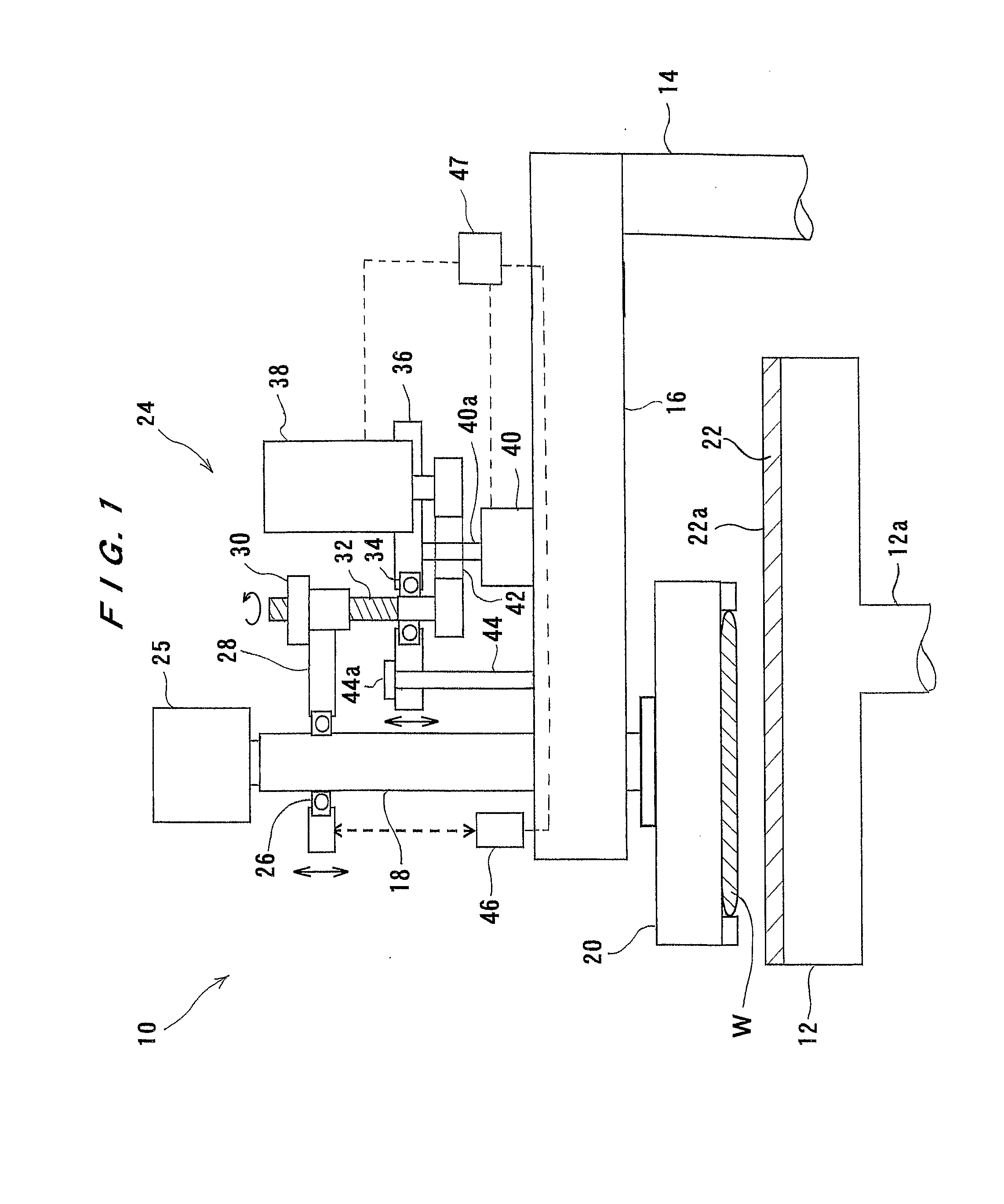
[0088]FIG. 4 is a schematic view showing a polishing apparatus 110 according to the present invention. As shown in FIG. 4, in the polishing apparatus 110 of the present embodiment, the top ring shaft 18 is vertically movable with respect to the top ring head 16 by a vertical movement mechanism 124. The vertical movement mechanism 124 has a first frame 128 supporting the top ring shaft 18 in a manner such that the top ring shaft 18 is rotatable via a bearing 126, a ball screw 132 threaded into a nut 130 mounted on the first frame 128, a second frame 136 fixed on the top ring head 16, and an AC servomotor 138 provided on the second frame 136 for rotating the ball screw 132. The controller 47 includes a current detector for detecting a current flowing through the servomotor 138. The controller 47 includes a storage device and a computer-readable medium having a program recorded therein for controlling the polishing apparatus 110.

[0089] The top ring shaft 18 is configured to be vertical...

third embodiment

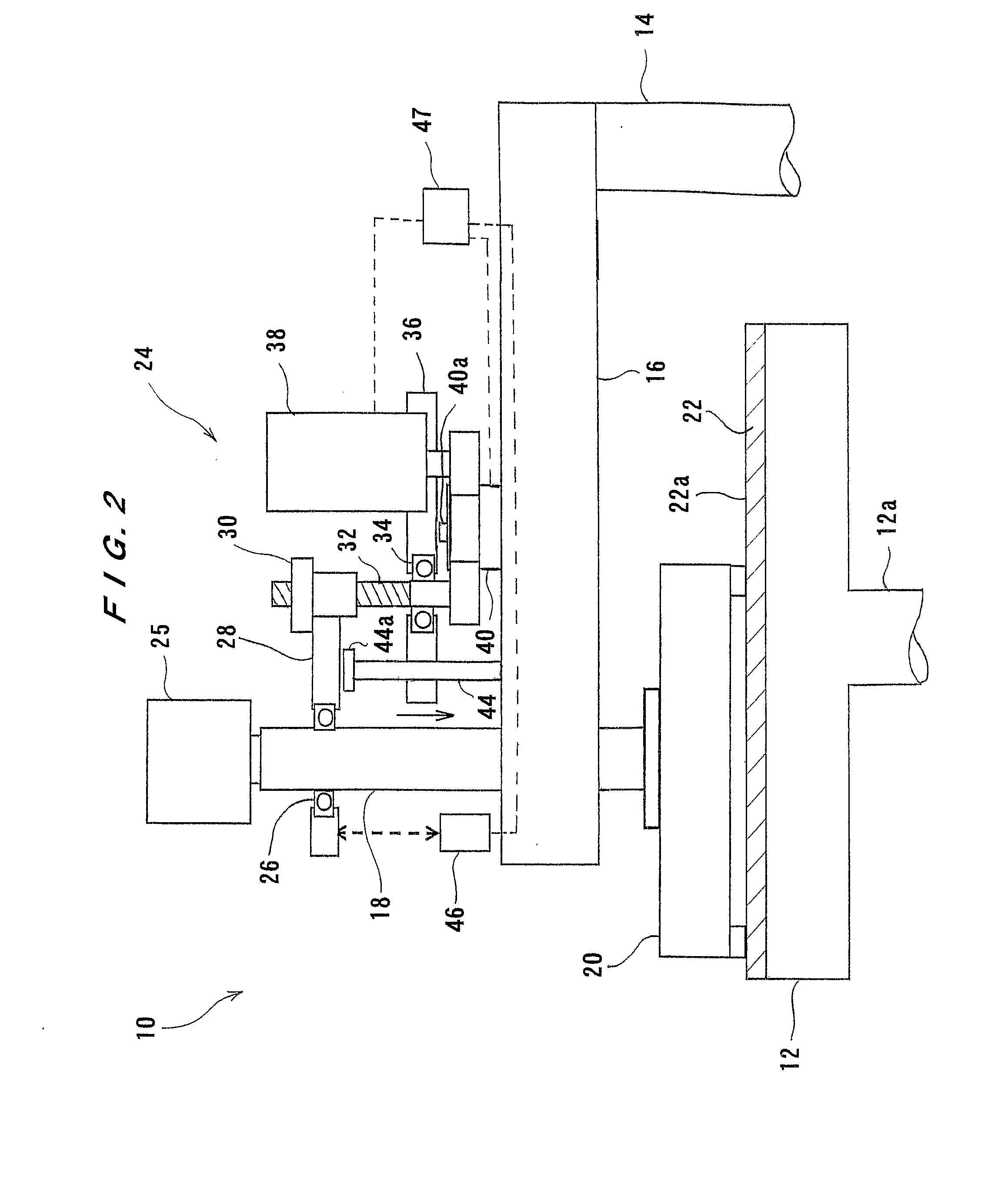
[0094]FIG. 6 is a schematic view showing a polishing apparatus 210 according to the present invention. As shown in FIG. 6, the polishing apparatus 210 in the present embodiment has a laser distance measuring sensor 246 for detecting the height of the polishing pad 22, a polishing liquid supply nozzle 251 for supplying slurry (polishing liquid) 250 onto the polishing pad 22, and an ejection nozzle 252 for ejecting nitrogen gas or air toward a surface of the polishing pad 22 to blow off the slurry 250 on the polishing pad 22. The distance measuring sensor 246 may comprise an ultrasonic distance measuring sensor.

[0095] With such an arrangement, the slurry 250 is removed from the polishing pad 22 by ejection of nitrogen gas or air. A laser can be applied from the laser distance measuring sensor 246 to a measurement portion from which the slurry 250 is removed. Accordingly, since the laser is not reflected on slurry or water on the polishing pad 22, it is possible to accurately detect a ...


PUM


Abstract

A polishing apparatus (1) has a polishing pad (22), a top ring (20) for holding a semiconductor wafer (W), a vertical movement mechanism (24) operable to move the top ring (20) in a vertical direction, a distance measuring sensor (46) operable to detect a position of the top ring (20) when a lower surface of the top ring (20) is brought into contact with the polishing pad (22), and a controller (47) operable to calculate an optimal position of the top ring (20) to polish the semiconductor wafer (W) based on the position detected by the distance measuring sensor (46). The vertical movement mechanism (24) includes a ball screw mechanism (30, 32, 38, 42) operable to move the top ring (20) to the optimal position.

Description

TECHNICAL FIELD [0001] The present invention relates to a polishing apparatus, and more particularly to a polishing apparatus for polishing a substrate such as a semiconductor wafer to a flat mirror finish. BACKGROUND ART [0002] In recent years, semiconductor devices have become more integrated, and structures of semiconductor elements have become more complicated. Further, the number of layers in multilayer interconnections used for a logical system has been increased. Accordingly, irregularities on a surface of a semiconductor device are increased, so that step heights on the surface of the semiconductor device tend to be large. This is because, in a manufacturing process of a semiconductor device, a thin film is formed on a semiconductor device, then micromachining processes, such as patterning or forming holes, are performed on the semiconductor device, and these processes are repeated to form subsequent thin films on the semiconductor device. [0003] When the number of irregular...

Claims


Application Information

Patent Timeline
IPC IPC(8): B24B49/00B24B51/00B24B29/00B24B5/00B24B37/30
CPCB24B37/30B24B47/22B24B49/16B24B37/105B24B37/005B24B37/10B24B49/00B24B37/32B24B49/18B24B37/042B24B49/183B24B37/20H01L21/304
Inventor NABEYA, OSAMUTOGAWA, TETSUJIFUKUSHIMA, MAKOTOYASUDA, HOZUMI
Owner EBARA CORP
Why Eureka
Try Eureka