

Thickness-measuring method during grinding process
a thin plate-like workpiece and thickness measurement technology, which is applied in the direction of manufacturing tools, semiconductor/solid-state device testing/measurement, lapping machines, etc., can solve the problems of excessive grinding of substrate and high degree of wear of probes on the chuck table side, so as to achieve accurate grinding of workpieces and suppress wear
- Summary
- Abstract
- Description
- Claims
- Application Information
AI Technical Summary
Benefits of technology
Problems solved by technology
Method used
Image

Examples
Embodiment Construction
[0023] Embodiments of the present invention will hereinafter be described with reference to the drawings.
[1] The Configuration and General Operation of a Grinding Machine
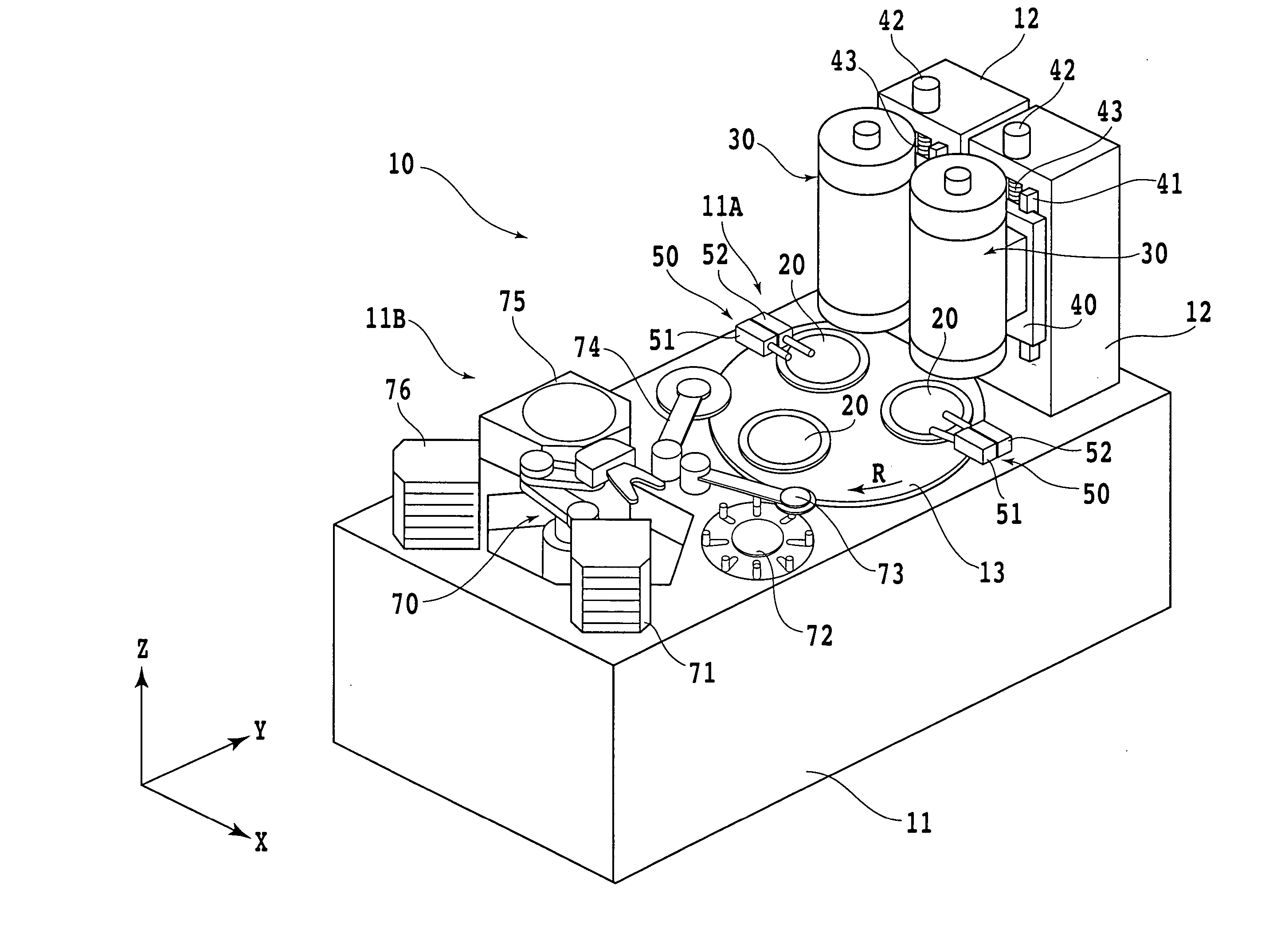
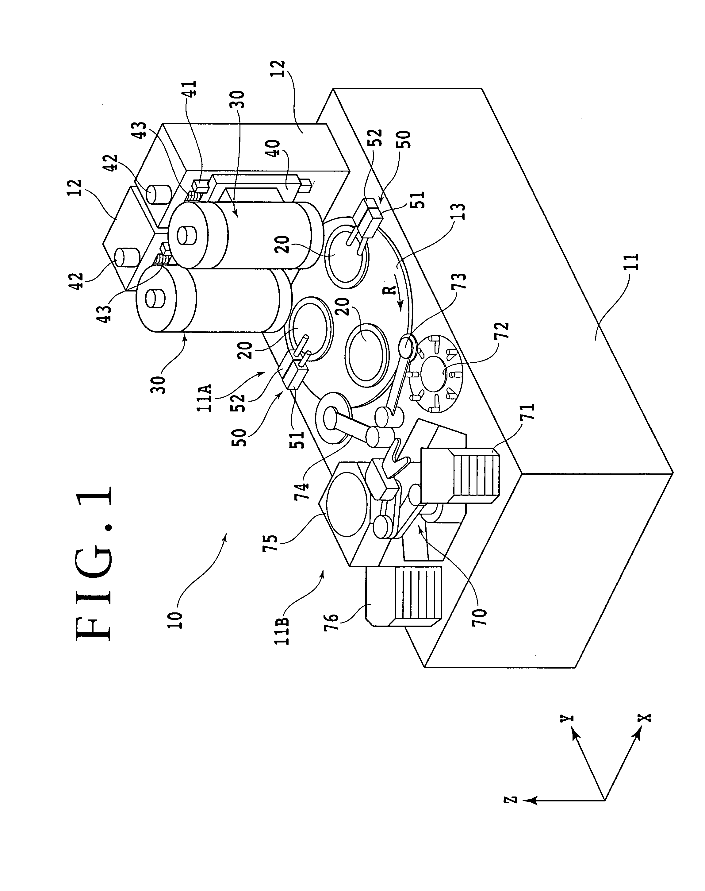
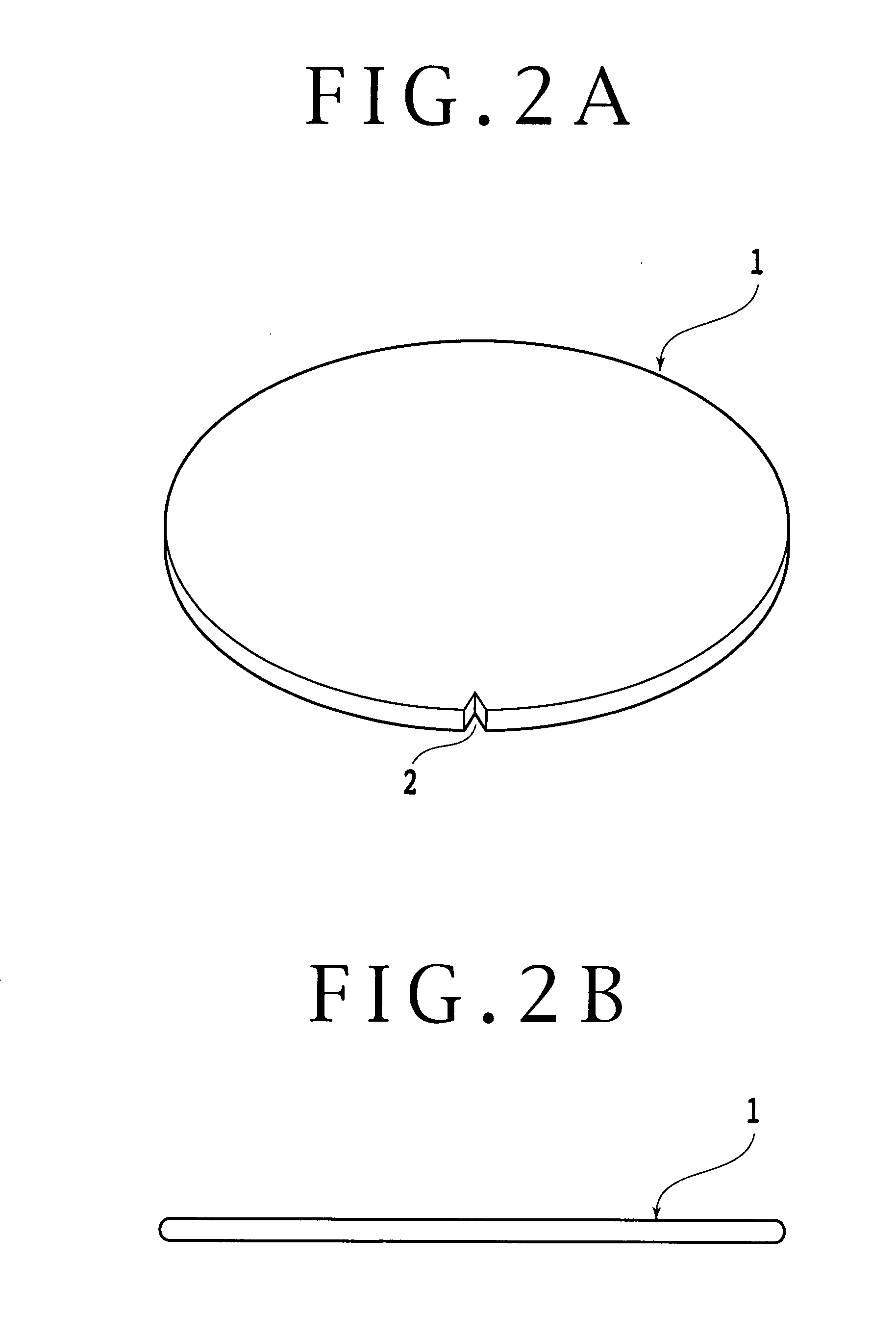
[0024]FIG. 1 illustrates a grinding machine 10 which grinds the surface of a workpiece, i.e., a semiconductor wafer (hereinafter, abbreviated as the wafer) such as a silicone wafer. FIGS. 2A and 2B illustrate a wafer to be ground. This wafer 1 is on a raw material stage in which a primary material, namely, an ingot is sliced, the sliced one is lapped to adjust its thickness, and then mechanically damaged layers formed on both surfaces of the lapped material are removed by etching. The wafer 1 is formed at its outer circumferential edge with a V-shaped notch 2 which designates crystal orientation. The wafer 1 has a thickness of e.g. about 700 μm, from which a thickness of, e.g. about 20 μm is removed by the grinding machine 10.
[0025] The grinding machine 10 illustrated in FIG. 1 includes a rectangular parallelepi...
PUM
| Property | Measurement | Unit |
|---|---|---|
| thickness | aaaaa | aaaaa |
| thickness | aaaaa | aaaaa |
| speed | aaaaa | aaaaa |
Abstract
Description
Claims
Application Information