Method for Fabricating Led Illumination Light Source and Led Illumination Light Source

a technology of led light source and led lamp, which is applied in the manufacture of electric discharge tubes/lamps, lighting and heating apparatuses, and discharge tubes luminescnet screens, etc. it can solve the problems of easy production of color unevenness, white light, and inability to produce color unevenness, so as to reduce color unevenness and eliminate color unevenness , the size and shape precision of the phosphor resin portion is sufficiently high, the effect of reducing color unevenness

Inactive Publication Date: 2008-03-27
SOVEREIGN PEAK VENTURES LLC
View PDF3 Cites 135 Cited by
  • Summary
  • Abstract
  • Description
  • Claims
  • Application Information

AI Technical Summary

Benefits of technology

[0044]In a method for fabricating an LED lamp according to the present invention, the step of forming an optical diffusion layer, in which particles to scatter the outgoing light of a phosphor resin portion (i.e., a diffusing agent) are dispersed, is performed between the step of forming the phosphor resin portion on a substrate such that an LED chip is covered with the phosphor resin portion and the step of arranging a lens that acts on the outgoing light of the phosphor resin portion. In this manner, an LED lamp that causes significantly reduced color unevenness can be fabricated more easily. That is to say, by forming a light-transmissive resin portion including a diffusing agent (i.e., the optical diffusion layer) to cover the phosphor resin portion, the light to be obliquely radiated from the phosphor resin portion as viewed from the LED chip (e.g., yellowish white light) can be scattered by the light-transmissive resin portion and mixed with light rays in the other colors, thus substantially eliminating the color unevenness. In addition, since the optical diffusion layer is formed after the phosphor resin portion has been formed, the method of making the phosphor resin portion itself does not have to be changed. That is why the LED lamp can be fabricated while keeping the size and shape precisions of the phosphor resin portion sufficiently high.
[0045]If a printing technique is adopted to carry out the process step of forming the phosphor resin portion and the process step of forming the optical diffusion layer, a lot of members can be formed at a time, which is beneficial for the manufacturer. Besides, if the printing technique is adopted in both of these process steps, the two process steps can be carried out continuously just by changing the stencils. As a result, the throughput increases and the optical diffusion layer that has a similar profile to that of the phosphor resin portion can be formed more easily.
[0046]In the LED lamp of the present invention, the optical diffusion layer is arranged so as to cover the phosphor resin portion and particles (i.e., a diffusing agent) are dispersed in the optical diffusion layer. Thus, the light rays radiated obliquely upward as viewed from the LED chip can be diffused and mixed with light rays in the other colors. Consequently, the color unevenness can be reduced significantly.

Problems solved by technology

An LED lamp of this type, however, easily produces color unevenness because the LED chip of each color has an excellent monochromatic peak.
That is to say, unless the light rays emitted from the respective LED chips are mixed together uniformly, color unevenness will be produced inevitably in the resultant white light.
However, the luminous flux of a single LED chip is too low.
As a result, unwanted color unevenness is produced.
However, the present inventors discovered that the color unevenness still persists in the prior art in the following situation.
However, even if one tries to form such a resin portion 113 with rounded corners by the printing technique, it is difficult to cut holes in such a shape through a printing stencil.
Thus, the holes cannot have the exactly intended shape.
As a result, the color unevenness could not be eliminated from the LED lamp as a whole.

Method used


Image

  • Method for Fabricating Led Illumination Light Source and Led Illumination Light Source
  • Method for Fabricating Led Illumination Light Source and Led Illumination Light Source
  • Method for Fabricating Led Illumination Light Source and Led Illumination Light Source

Examples


Embodiment Construction

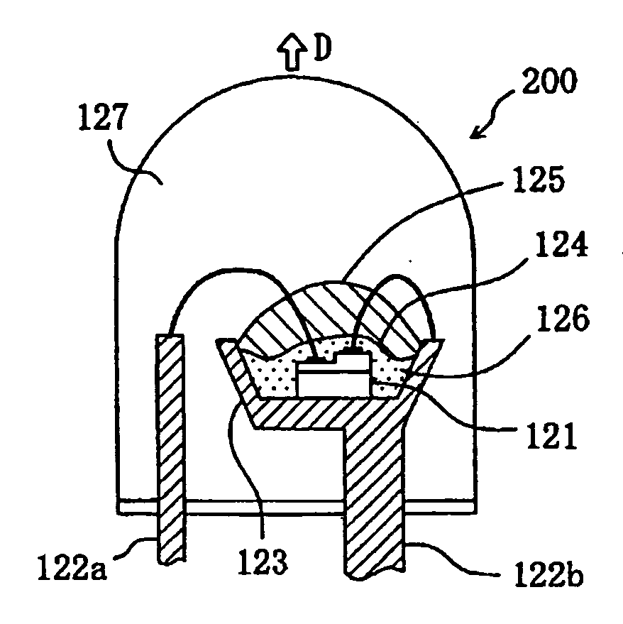
[0076]While looking for a good idea for minimizing the color unevenness to be produced by an LED lamp, it occurred to the present inventors that the color unevenness should be reduced significantly if the light radiated obliquely upward (in yellowish white) was scattered and mixed with the other light rays producing color white. However, if a method of making a structure that causes such scattering were too complicated, then the mass productivity of LED lamps would decline and the manufacturing cost thereof would rise. For that reason, the color unevenness is preferably minimized by using as simple a structure as possible. In view of this consideration, the present inventors discovered that the color unevenness could be reduced effectively by covering the phosphor resin portion with a light-transmissive resin portion in which a diffusing agent is dispersed as fine particles (i.e., an optical diffusion layer), thus acquiring the basic idea of the present invention.

[0077]An LED lamp a...


PUM


Abstract

An LED lamp according to the present invention includes: at least one LED chip 12 that is mounted on a substrate 11; a phosphor resin portion 13 that covers the LED chip 12; a lens 22 to act on the outgoing light of the phosphor resin portion 13; and an optical diffusion layer (light-transmissive resin portion 20), which is arranged between the phosphor resin portion 13 and the lens 22 and in which particles to scatter the light are dispersed.

Description

TECHNICAL FIELD[0001]The present invention relates to a method for fabricating an LED lamp and to an LED lamp and more particularly relates to a method for fabricating a white LED lamp that can be used as general illumination and to a white LED lamp.BACKGROUND ART[0002]A light emitting diode (which will be referred to herein as an “LED chip”) is a semiconductor device that can radiate an emission in a bright color with high efficiency even though its size is small. The emission of an LED chip has an excellent monochromatic peak. To produce white light from LED chips, a conventional LED lamp arranges red, green and blue LED chips close to each other and gets the light rays in those three different colors diffused and mixed together. An LED lamp of this type, however, easily produces color unevenness because the LED chip of each color has an excellent monochromatic peak. That is to say, unless the light rays emitted from the respective LED chips are mixed together uniformly, color une...

Claims


Application Information

Patent Timeline
Patent Type & Authority Applications(United States)
IPC IPC(8): H01J1/00H01J9/02F21Y101/02H01L33/32H01L33/50H01L33/54H01L33/56H01L33/60H01L33/62
CPCF21K9/00F21S6/00F21S6/003F21Y2101/02H01L33/50F21Y2105/001H01L2933/0091H01L33/56H01L2224/48091H01L2924/00014F21Y2105/10F21Y2115/10F21K9/64
Inventor YANO, TADASHITAKAHASHI, KIYOSHISHIMIZU, MASANORI
Owner SOVEREIGN PEAK VENTURES LLC
Why Eureka
Try Eureka