Self-Calibrating Optical Emission Spectroscopy for Plasma Monitoring

a technology of optical emission spectroscopy and plasma monitoring, which is applied in the field of plasma processing, can solve the problems of processing system downtime, affecting the accuracy of optical measurements, and high cost, and achieve the effect of improving the simplicity and reliability of instruments, improving accuracy and usefulness, and prolonging the time between window servicing

Inactive Publication Date: 2008-04-03
TOKYO ELECTRON LTD
View PDF3 Cites 20 Cited by
  • Summary
  • Abstract
  • Description
  • Claims
  • Application Information

AI Technical Summary

Benefits of technology

[0011]An objective of the present invention is to improve the simplicity and reliability of the instrumentation, the length of the time between window servicing, and the accuracy and usefulness, of optical emission spectroscopy in the monitoring of plasma processes, particularly those used in the manufacture of semiconductors and other related products.

Problems solved by technology

Such deposits affect the window transparency and the radiation being monitored, and can affect the accuracy of the optical measurements if the change in window transparency is not considered.
Such window maintenance involves processing system down-time, which is expensive.

Method used


Image

  • Self-Calibrating Optical Emission Spectroscopy for Plasma Monitoring
  • Self-Calibrating Optical Emission Spectroscopy for Plasma Monitoring

Examples


Embodiment Construction

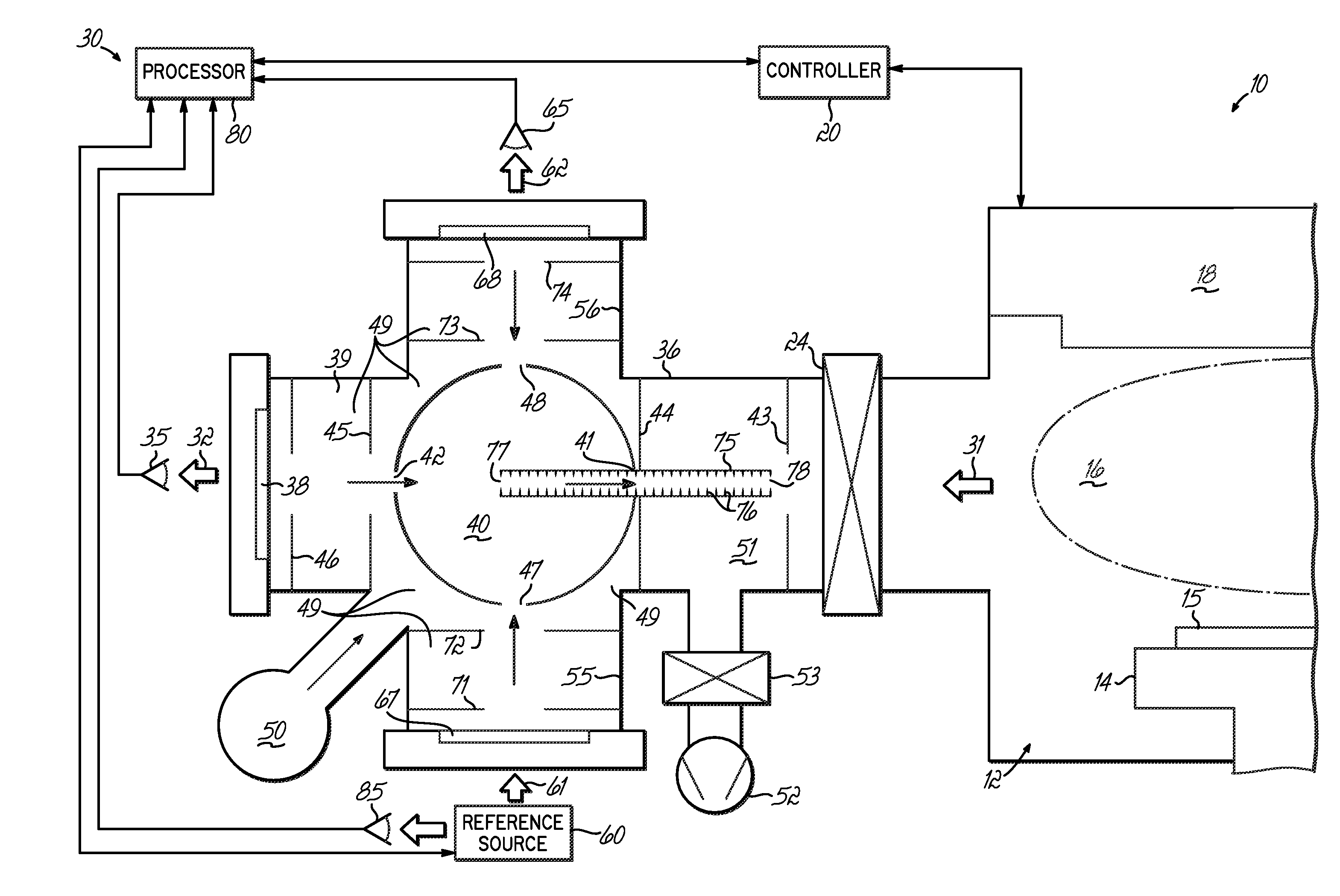
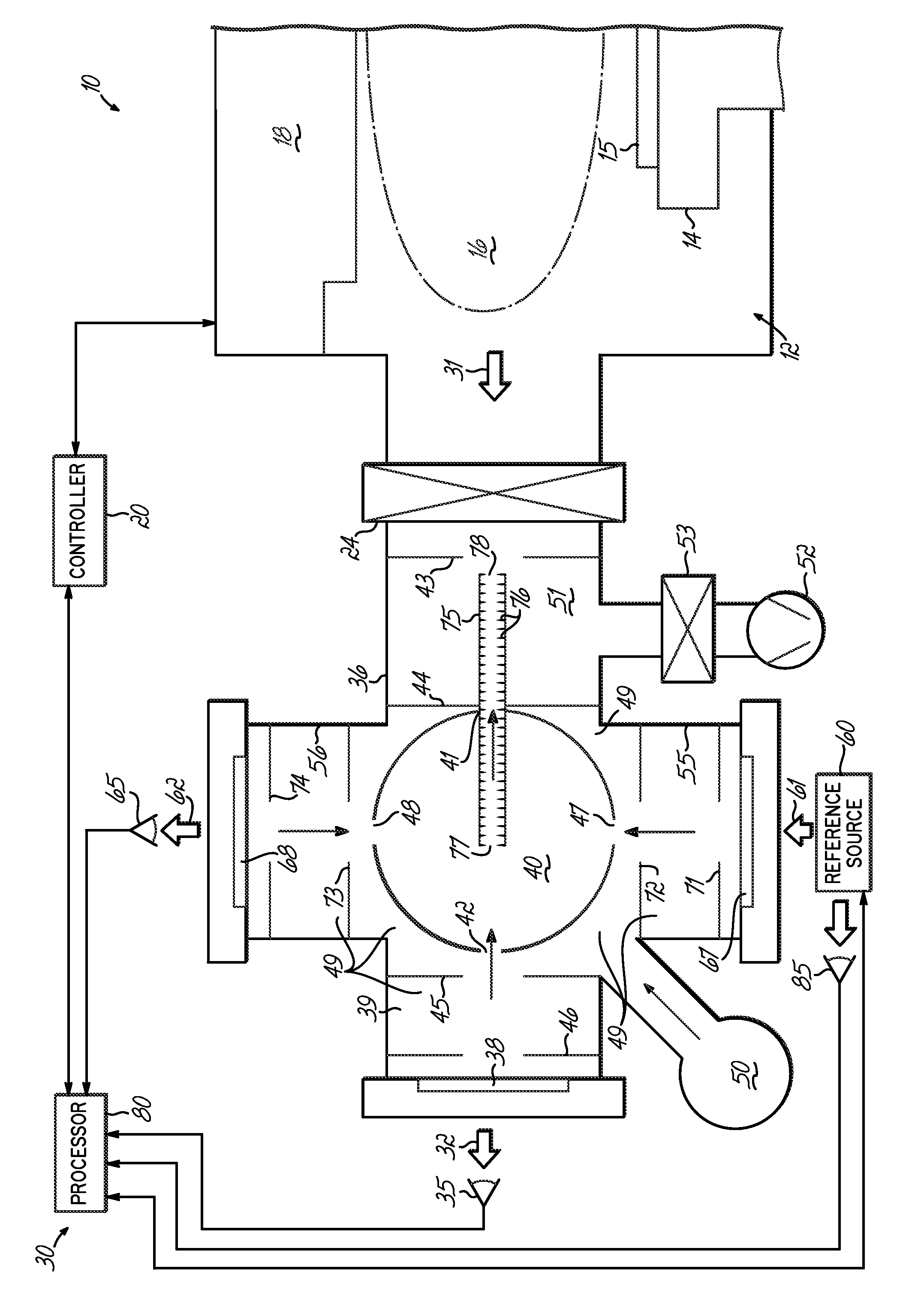
[0022]The FIGURE diagrammatically illustrates a plasma processing system 10 of the type used for processing semiconductors and other related substrates. The system 10 includes a vacuum chamber 12 in which is situated a substrate holder 14 on which may be mounted a semiconductor wafer 15 for processing. A plasma source is provided within the chamber 12 to energize a plasma 16 in process gas maintained under vacuum within the chamber 12. The plasma source can include a pair of electrodes, which can include the holder 14 and a sputtering target or other electrode 18, or can include some other plasma generating system, for example an inductively coupled plasma (ICP) source that typically includes an RF inductive or capacitive electrode coupled to the plasma from inside or outside of the chamber 12. A programmed controller 20 is typically provided to maintain reliable and repeatable operation of the apparatus 10 and to precisely control the process.

[0023]To monitor the condition of the p...


PUM

PropertyMeasurementUnit
volumeaaaaaaaaaa
exhaust volumeaaaaaaaaaa
plasma emissionsaaaaaaaaaa

Abstract

A plasma processing system and plasma monitor therefor is provided in which a plasma monitor housing is coupled to a plasma processing chamber such that a line-of-sight monitoring path extends through the housing to an optical sensor outside of a window. A separate reference signal path extends through the housing from a reference light source on one side of the housing to a reference optical sensor on the other side of the housing. The housing is configured so that deposits from the chamber affect all of the windows equally, and to retard the flow of contaminating film forming material onto the windows, using, for example, baffles, gas counterflow, and a balanced radial-leg housing. A processor uses the reference signal to determine window contamination and compensate for signal attenuation along the monitoring path caused by window coating, in the making of a measurement of plasma emissions. The measurement can be used by the processing system to control the plasma.

Description

[0001]This application is related to U.S. patent application Ser. No. 11 / 082,223, filed Mar. 17, 2005, which is a continuation of International Application No. PCT / US03 / 26208, filed Aug. 21, 2003, which claims priority to U.S. Provisional Application No. 60 / 414,348, filed Sep. 30, 2002, the contents of all of which are hereby expressly incorporated herein by reference.[0002]This application is also related to U.S. patent application Ser. No. 11 / 082,246, filed Mar. 17, 2005, which is a continuation of International Application No. PCT / US03 / 30051, filed Sep. 25, 2003, which claims priority to U.S. Provisional Application No. 60 / 414,349, filed Sep. 30, 2002, the contents of all of which are hereby expressly incorporated herein by reference.FIELD OF INVENTION[0003]This invention relates to plasma processing, and particularly to plasma monitoring of the plasma in vacuum chambers of plasma processing systems.BACKGROUND OF THE INVENTION[0004]Plasma processes are widely used for applying an...

Claims


Application Information

Patent Timeline
Patent Type & Authority Applications(United States)
IPC IPC(8): H01L21/306C23F1/00C23C16/00
CPCC23C14/52C23C14/54H01J37/32972G01N21/68H01J37/32935C23C16/54
Inventor VUKOVIC, MIRKO
Owner TOKYO ELECTRON LTD
Why Eureka
Try Eureka