

Manufacturing method for semiconductor device, semiconductor device, substrate processing system, program and memory medium
a manufacturing method and semiconductor technology, applied in semiconductor devices, semiconductor/solid-state device details, coatings, etc., can solve the problems of easy increased dielectric constant, and increased parasitic capacity of the interlayer insulation film that covers the wiring, so as to prevent the damage to the interlayer insulation film, the effect of improving the reliability of the wiring
- Summary
- Abstract
- Description
- Claims
- Application Information
AI Technical Summary
Benefits of technology
Problems solved by technology
Method used
Image

Examples
Embodiment Construction
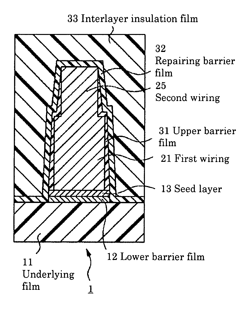
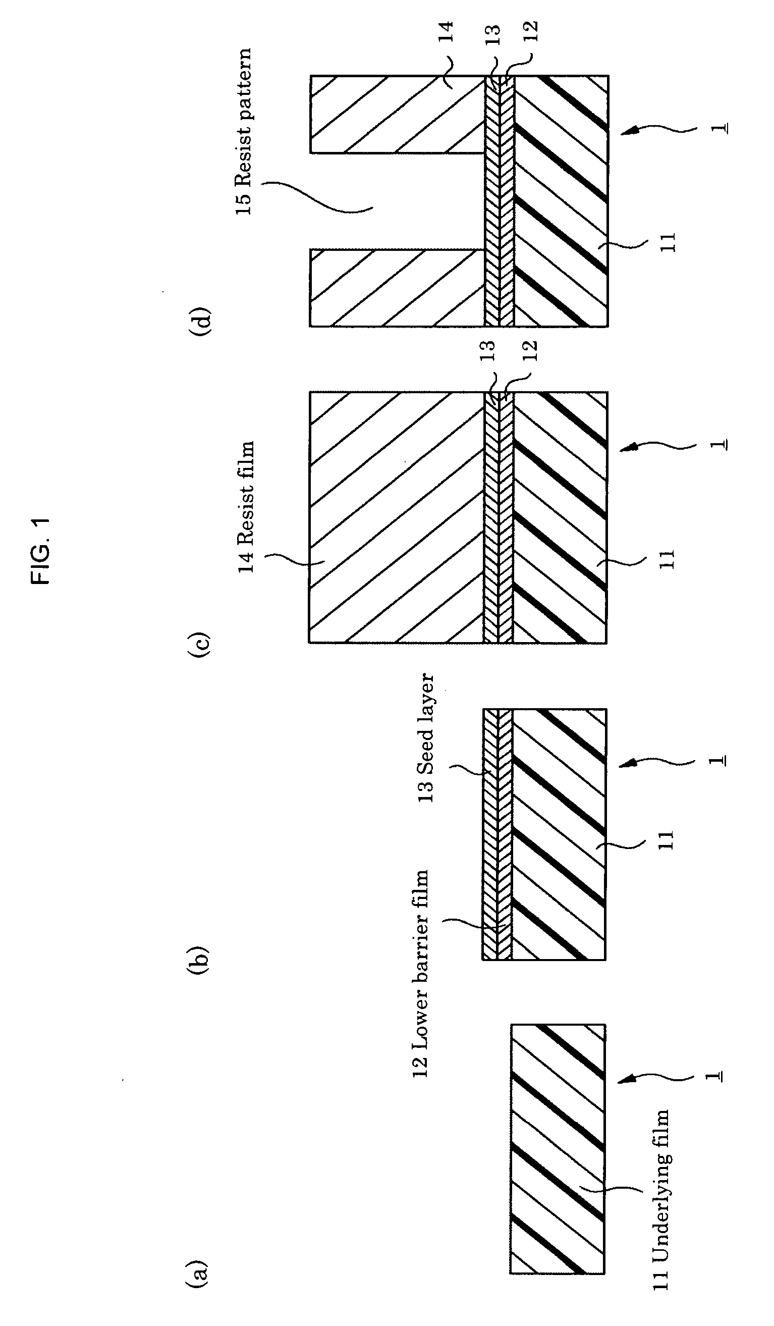
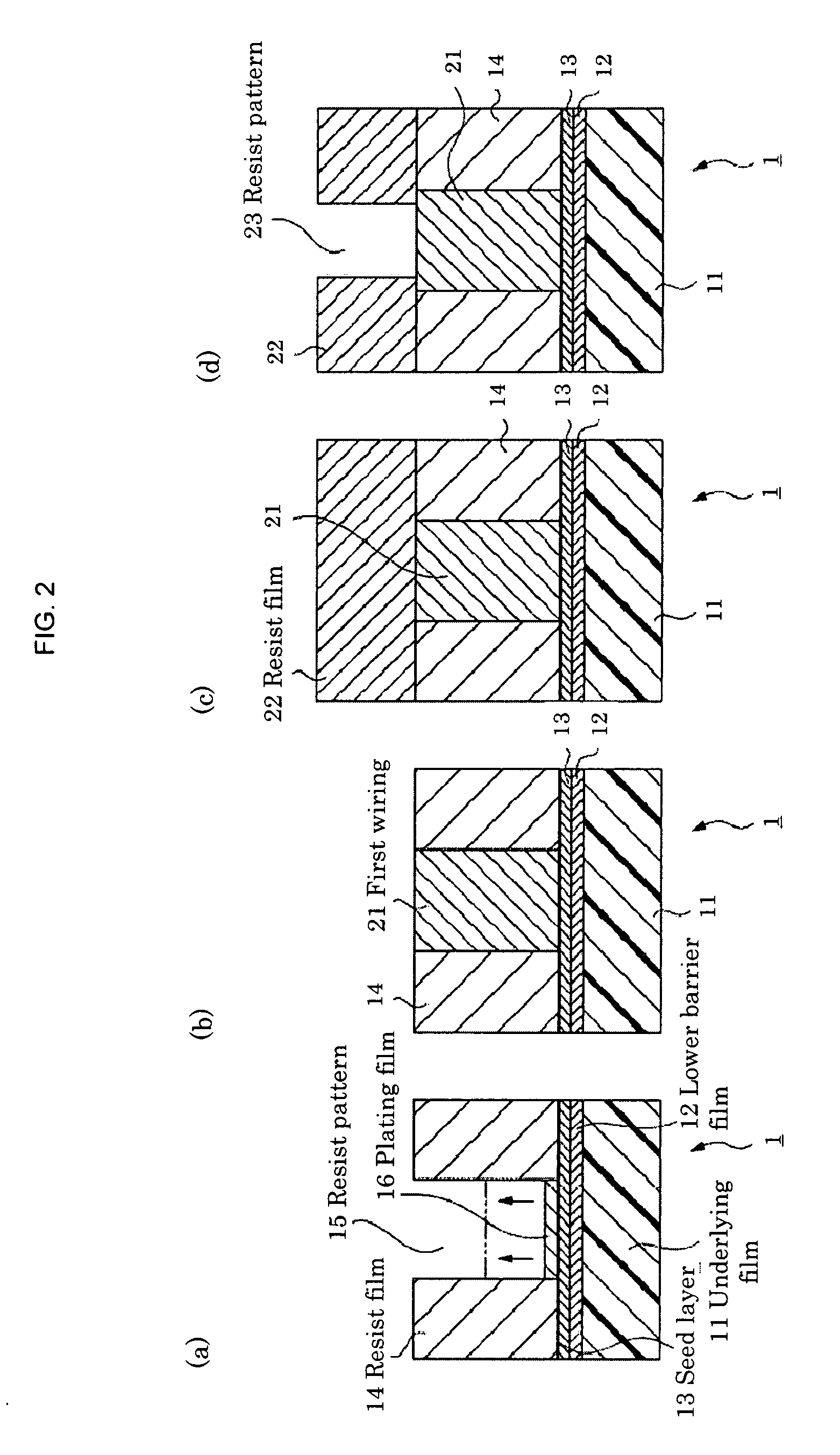
[0031]A dual damascene process, an embodiment of a manufacturing method of a semiconductor device according to the present invention, is explained referring to FIGS. 1 to 5. 1 in FIG. 1 (a) is a substrate (underlying substrate) which has an underlying film 11, and, for example, a semiconductor element (not shown), such as a transistor, is formed thereon.
(Step 1: Forming of a Lower Barrier Film 12 and a Seed Layer 13)
[0032]First, as shown in FIG. 1 (b), a lower barrier film 12 is formed, which is a lower diffusion barrier film consisting of, for example, conductive TiN (titanium nitride), on an underlying film 11, and then a seed layer 13 is formed, consisting of, for example Cu (copper) on the lower barrier film 12. The lower barrier film 12 is a lower diffusion barrier film to prevent a metal which consists a wiring in a subsequent process and a metal which consists of the seed layer 13 from diffusing onto the underlying film 11, and the seed layer 13 functions as an electrode when...
PUM
 Abstract
Description
Claims
Application Information