Method for leakage reduction in fabrication of high-density FRAM arrays

a high-density fram array and leakage reduction technology, applied in the field of cleaning the structure of etched ferroelectric capacitors, can solve the problems of degrading the polarization performance of ferroelectric cell capacitors and unacceptable leakage levels

Active Publication Date: 2008-04-03
TEXAS INSTR INC
View PDF9 Cites 46 Cited by
  • Summary
  • Abstract
  • Description
  • Claims
  • Application Information

AI Technical Summary

Problems solved by technology

However, conventional ferroelectric cell fabrication techniques often lead to unacceptable levels of leakage and degraded polarization performance of ferroelectric cell capacitors, particularly for scaled smaller capacitor dimensions, whereby there is a need for improved methods for ferroelectric capacitor fabrication in the manufacture of semiconductor devices.

Method used


Image

  • Method for leakage reduction in fabrication of high-density FRAM arrays
  • Method for leakage reduction in fabrication of high-density FRAM arrays
  • Method for leakage reduction in fabrication of high-density FRAM arrays

Examples


Embodiment Construction

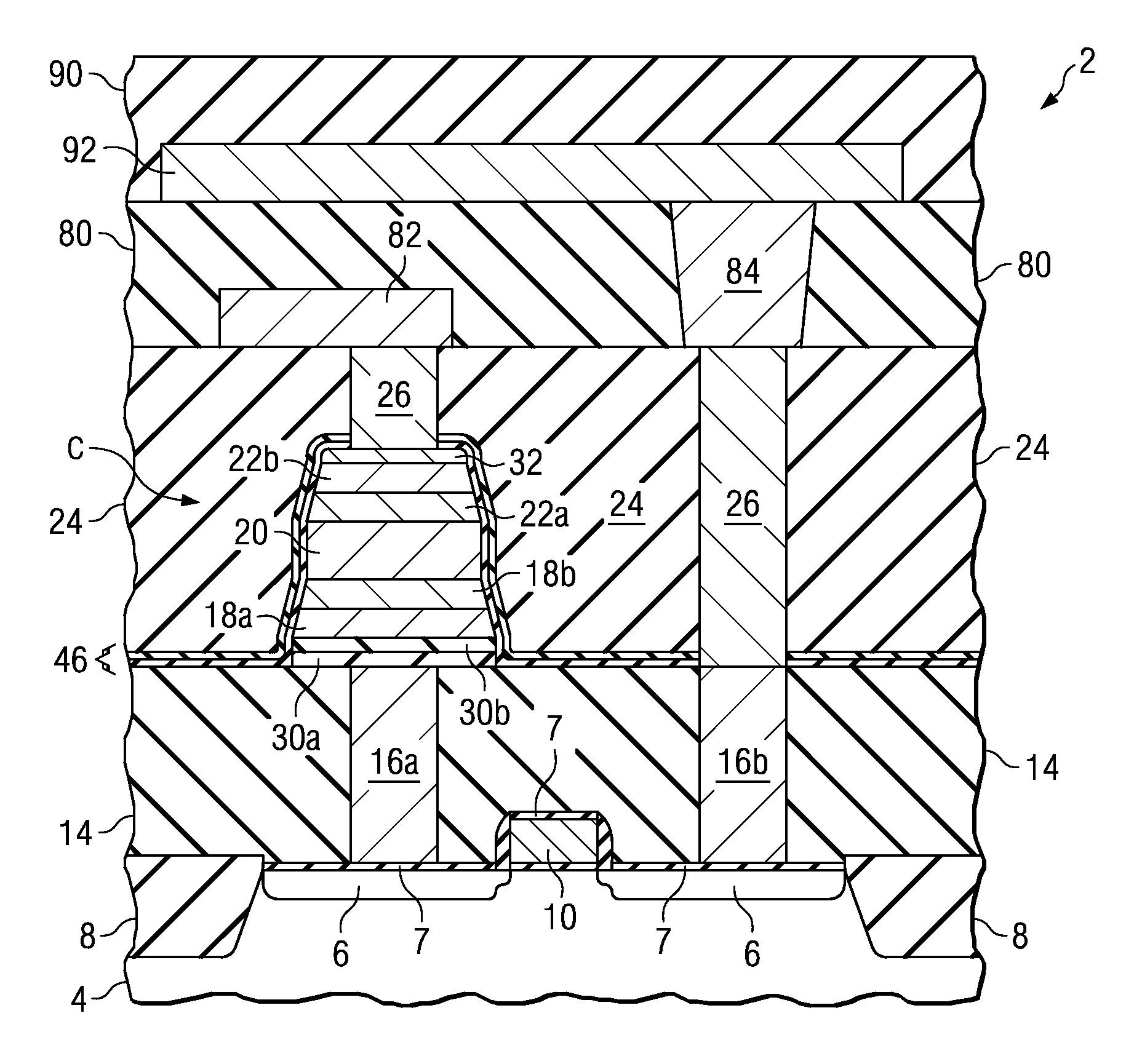
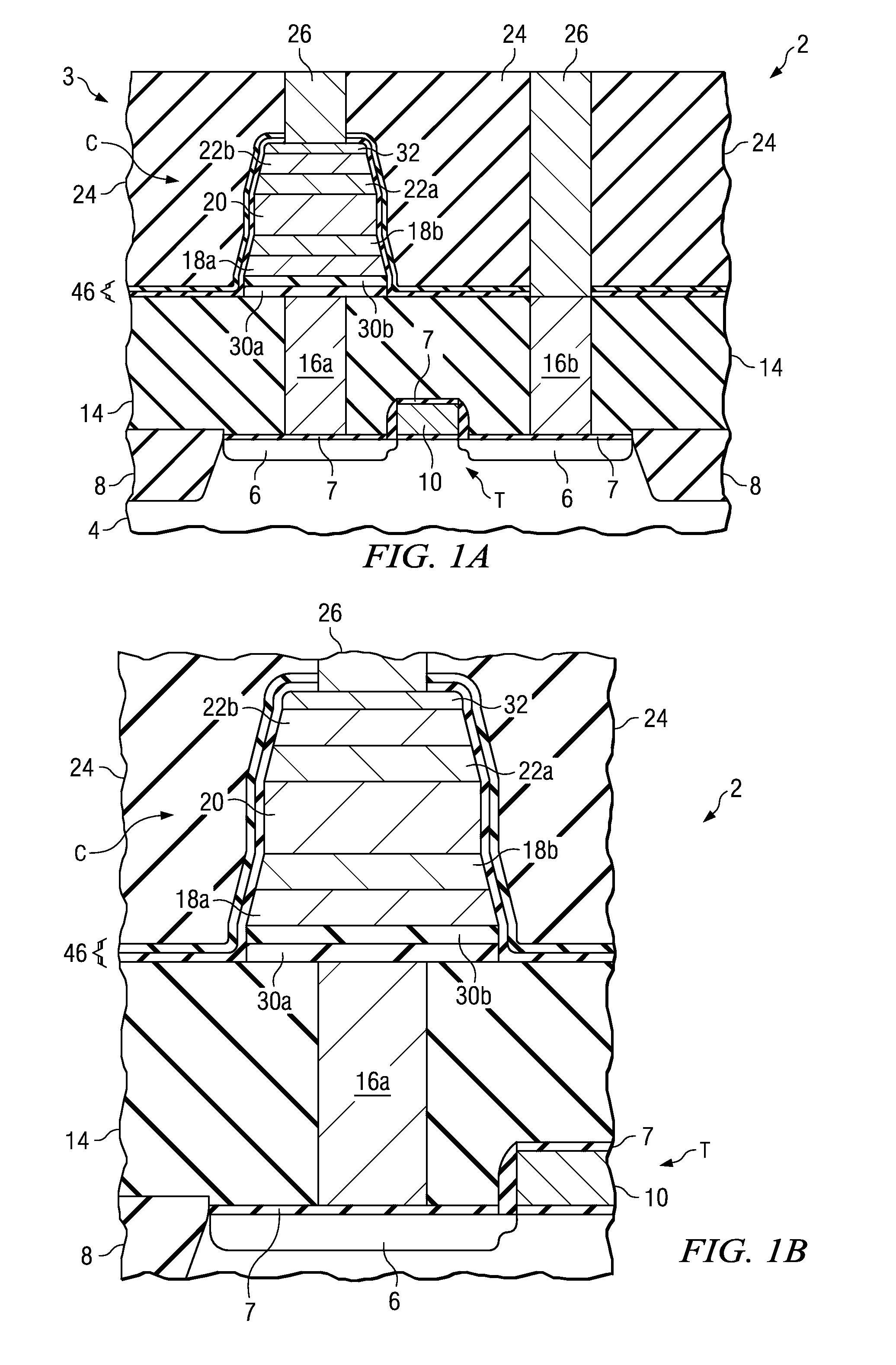
[0013]The invention will now be described with reference to the attached drawing figures, wherein like reference numerals are used to refer to like elements throughout. The invention relates to the use of water-containing post stack etch (PSE) processes and wet-cleaning of etched ferroelectric capacitor stack structures, by which capacitor leakage may be mitigated in the fabrication of semiconductor devices, for example, devices having memory cells with ferroelectric cell capacitors or other devices, such as integrated circuits, in which ferroelectric capacitors are used. The various aspects and advantages of the invention are hereinafter illustrated and described in conjunction with the drawings, wherein the illustrated structures are not necessarily drawn to scale.

[0014]FIGS. 1A and 1B illustrate an exemplary ferroelectric memory cell (1T1C) with a cell transistor T and a ferroelectric capacitor C in a semiconductor device 2 formed in a wafer comprising a silicon substrate 4 in ac...


PUM

PropertyMeasurementUnit
temperatureaaaaaaaaaa
thicknessaaaaaaaaaa

Abstract

A method is provided for fabricating a ferroelectric capacitor structure including a method for etching and cleaning patterned ferroelectric capacitor structures in a semiconductor device. The method comprises etching portions of an upper electrode, etching ferroelectric material, and etching a lower electrode to define a patterned ferroelectric capacitor structure, and etching a portion of a lower electrode diffusion barrier structure. The method further comprises ashing the patterned ferroelectric capacitor structure using a first ashing process, where the ash comprises an oxygen/nitrogen/water-containing ash, performing a wet clean process after the first ashing process, and ashing the patterned ferroelectric capacitor structure using a second ashing process.

Description

REFERENCE TO RELATED APPLICATIONS[0001]This application claims priority to Ser. No. 60 / 877,299 filed Dec. 27, 2006, which is entitled “Method for Leakage Reduction in Fabrication of High-Density FRAM Arrays.”FIELD OF INVENTION[0002]The invention relates generally to semiconductor devices and more particularly to methods for cleaning etched ferroelectric capacitor structures in the fabrication of semiconductor devices.BACKGROUND OF THE INVENTION[0003]Memory systems are used for storage of data, program code, and / or other information in many electronic products, such as personal computer systems, embedded processor-based systems, video image processing circuits, portable phones, and the like. Ferroelectric memory, sometimes referred to as “FRAM” or “FERAM”, is a non-volatile form of memory commonly organized in single-transistor, single-capacitor (1T1C) or two-transistor, two-capacitor (2T2C) cell configurations, in which each memory cell includes one or more pairs of access transisto...

Claims


Application Information

Patent Timeline
Patent Type & Authority Applications(United States)
IPC IPC(8): H01L21/00
CPCH01L27/11507H01L28/75H01L28/55H10B53/30
Inventor CELII, FRANCIS GABRIELUDAYAKUMAR, KEZHAKKEDATH R.SHINN, GREGORY B.MOISE, THEODORE S.SUMMERFELT, SCOTT R.
Owner TEXAS INSTR INC
Why Eureka
Try Eureka