Pulsed plasma etching method and apparatus

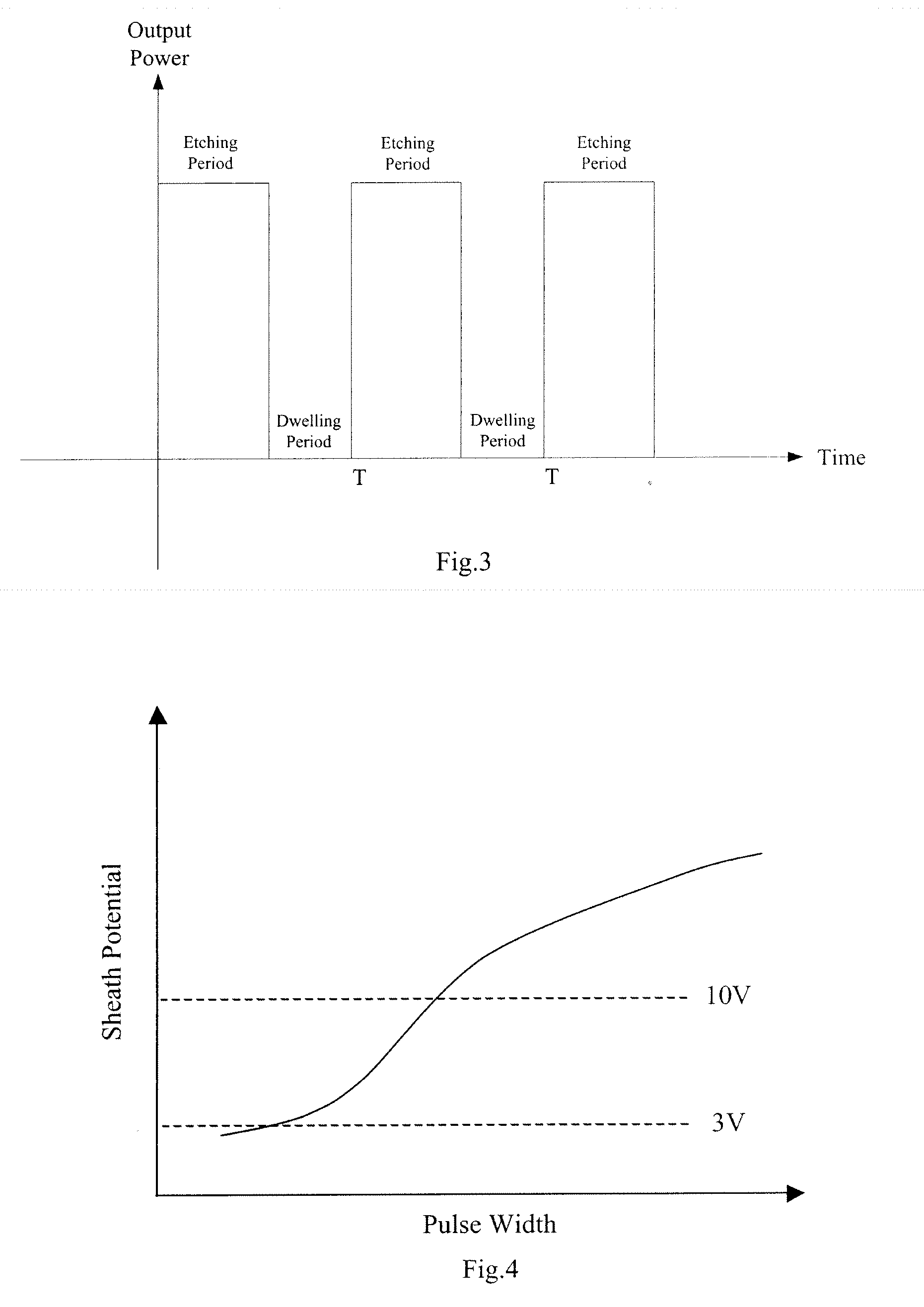
a plasma etching and plasma technology, applied in the direction of electrical equipment, basic electric elements, electric discharge tubes, etc., can solve the problems of serious potential risk of continuous energy output control of etch termination, serious loss of silicon (si loss or si recess) in the aa region, ldd region, etc., to improve the precision of an endpoint

Inactive Publication Date: 2008-04-03
SEMICON MFG INT (SHANGHAI) CORP
View PDF7 Cites 249 Cited by
  • Summary
  • Abstract
  • Description
  • Claims
  • Application Information

AI Technical Summary

Benefits of technology

[0009]In view of the above, an object of the invention is to provide a plasma etching method and apparatus which can improve the precision of an endpoint where the etching can be disabled.
[0027]The plasma etching method and apparatus can output power in a pulse mode, that is, the RF power source for generating plasma outputs RF power in a pulse mode, and the etching gas is ionized in a pulse mode to generate the plasma. Further, a film layer to be etched can be etched by the plasma in an intermittent not continuous mode, and thus the etching effect of the plasma can be controlled and buffered. With such a pulse plasma etching mode, a proportion of the time width in which the plasma source outputs power relative to the whole pulse period can be adjusted as needed. That is, during the whole etching phase, an etching interval of time for the plasma can be set as needed, and the electron temperature and the sheath voltage of the plasma can be adjusted to be within an appropriate range. During an etching process for a semiconductor device of 65 nm and below, the inventive plasma etching method and apparatus can precisely control an etching depth and improve the precision of a point where the etching can be disabled. The etching depth can be controlled precisely during a process such as the stripping of the photoresist, the etching of the gate oxide layer, etc., thus resulting in elimination of any recess occurring in the active area and the LDD region.

Problems solved by technology

Such a continuous energy output has a serious potential risk in a control of etch termination.
Moreover, during the stripping of the photoresist layer through the oxygen plasma that is output continuously, the oxygen plasma tends to penetrate the gate oxide layer, and further enters the active area and reacts with the silicon under the gate oxide layer to generate silicon oxide, which can be stripped in a subsequent wet-cleaning process, resulting in a serious loss of silicon (Si loss or Si recess) in the AA region.
However, for a device of 65 nm and below, the thickness of the gate oxide layer is only approximately 10 Å, and an LDD depth is below approximately 250 Å. In this case, the recess resulted from the Si loss can destroy the LDD region and may seriously impair the performance of the device.

Method used


Image

  • Pulsed plasma etching method and apparatus
  • Pulsed plasma etching method and apparatus
  • Pulsed plasma etching method and apparatus

Examples


Embodiment Construction

[0036]In order to make the above objects, characteristics and advantages of the invention more apparent, preferred embodiments of the invention will be described in detail with reference to the drawings.

[0037]Details will be presented in the following for a full understanding of the invention. However, the invention can be implemented in any way different from those disclosed here, and variations and modifications thereto can be obvious to those skilled in the art without departing from the scope of the invention. Note that the invention shall not be limited to the disclosed embodiments in the following.

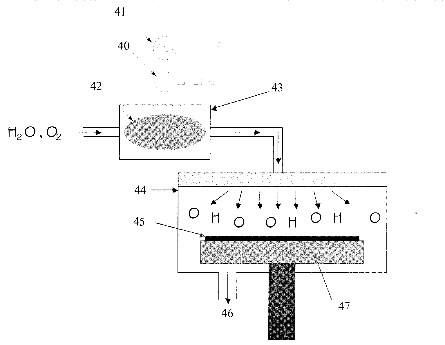
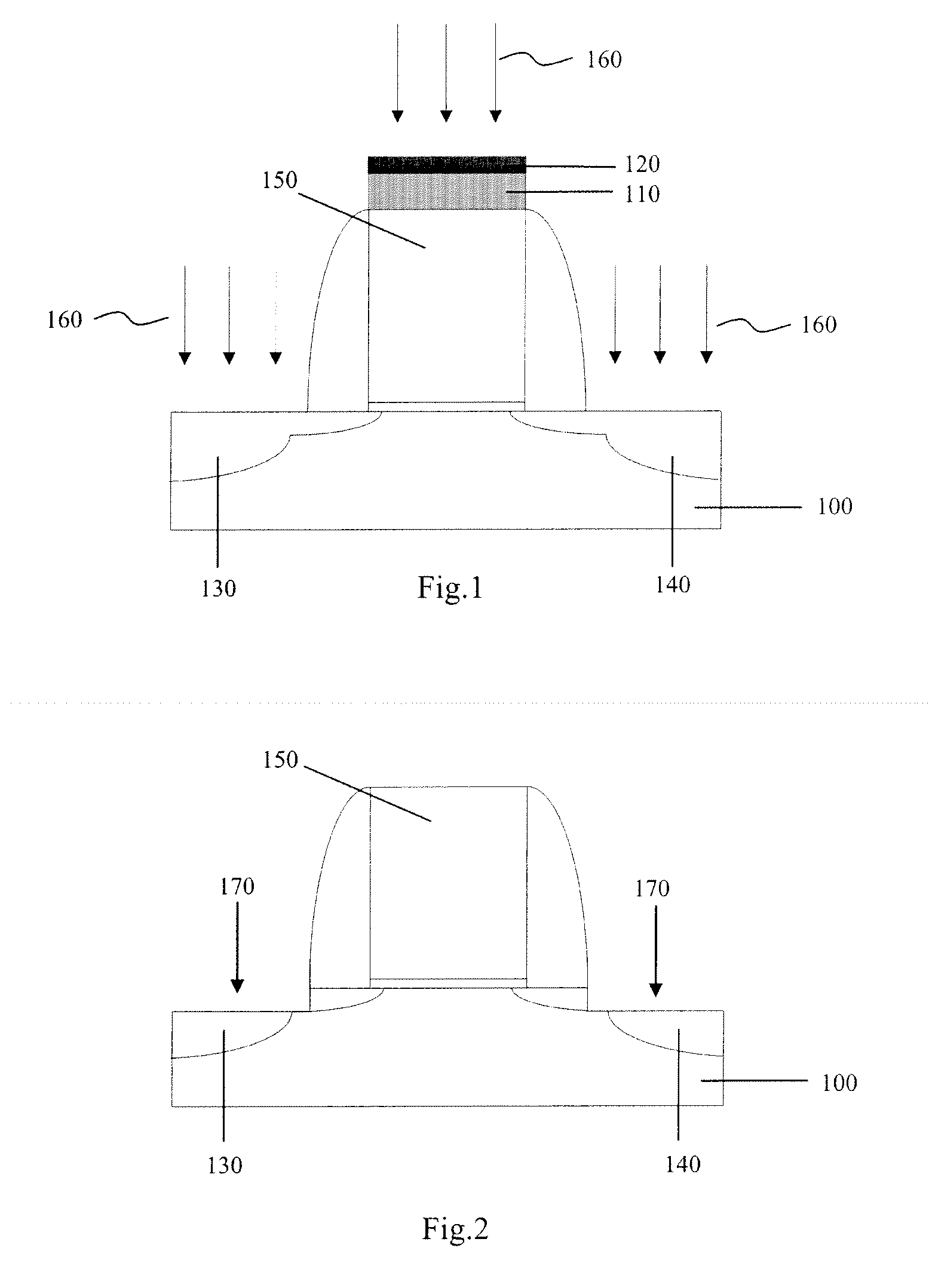
[0038]A plasma etching process is important for semiconductor manufacturing technologies, and can be used for etching a medium layer including a silicon oxide layer, a silicon nitride layer, a polysilicon layer, etc., and a material with a high dielectric constant such as hafnium oxide, hafnium silicon oxide, hafnium silicon oxynitride, etc., for etching a metal layer such as copper,...


PUM

PropertyMeasurementUnit
poweraaaaaaaaaa
pressureaaaaaaaaaa
temperatureaaaaaaaaaa

Abstract

A plasma etching method includes preparing in a reaction chamber a semiconductor substrate on which a material layer to be etched is provided; and injecting an etching gas into the reaction chamber, the etching gas being ionized through an RF (Radio Frequency) power source to generate a plasma, wherein the RF power source outputs RF power in a pulse output mode. The plasma etching apparatus includes a reaction chamber adapted to contain an etching gas; and an RF power source adapted to output RF power for excitation of the etching gas to generate plasma, wherein the apparatus further include a pulse control circuit adapted to control the RF power source to output RF power in a pulse output mode. With the invention, the plasma for etching can be generated in a pulse output mode, thus improving a precision of an endpoint where the etching can be disabled.

Description

[0001]This application claims the priority of Chinese Patent Application No. 200610116855.6, filed Sep. 30, 2006, the entire disclosure of which is incorporated herein by reference.FIELD OF THE INVENTION[0002]The present invention relates to the field of semiconductor integrated circuit manufacturing technologies, and in particular to a plasma etching method and apparatus.BACKGROUND OF THE INVENTION[0003]As semiconductor manufacturing technologies advance rapidly, integrated circuits tend to have a more rapid operational rate, a larger data storage capacity and more functions. Semiconductor wafers are striding forward to a higher component density and a high integration level. A characteristic dimension of a gate line width of a semiconductor device, such as a MOS (Metal Oxide Semiconductor) device, becomes thinner, and a length thereof becomes shorter.[0004]In a process of manufacturing a metal oxide semiconductor device, an insulation layer such as a silicon oxide film or a silico...

Claims


Application Information

Patent Timeline
Patent Type & Authority Applications(United States)
IPC IPC(8): H01L21/306
CPCH01J37/32137H01J37/32357H01L21/32137H01L21/31122H01L21/32136H01L21/31116
Inventor WU, HANMING
Owner SEMICON MFG INT (SHANGHAI) CORP
Why Eureka
Try Eureka