

Rectifier circuit, semiconductor device using the rectifier circuit, and driving method thereof
a rectifier circuit and rectifier circuit technology, applied in emergency protective circuit arrangements, near-field systems using receivers, instruments, etc., can solve the problems of reducing the amplitude of ac voltage, mismatching of impedance, etc., to prevent deterioration or destruction of semiconductor elements in rectifier circuits due to excess current, improve reliability of semiconductor devices, and prevent deterioration or destruction of semiconductor elements due to excess current
- Summary
- Abstract
- Description
- Claims
- Application Information
AI Technical Summary
Benefits of technology
Problems solved by technology
Method used
Image

Examples
embodiment mode 1
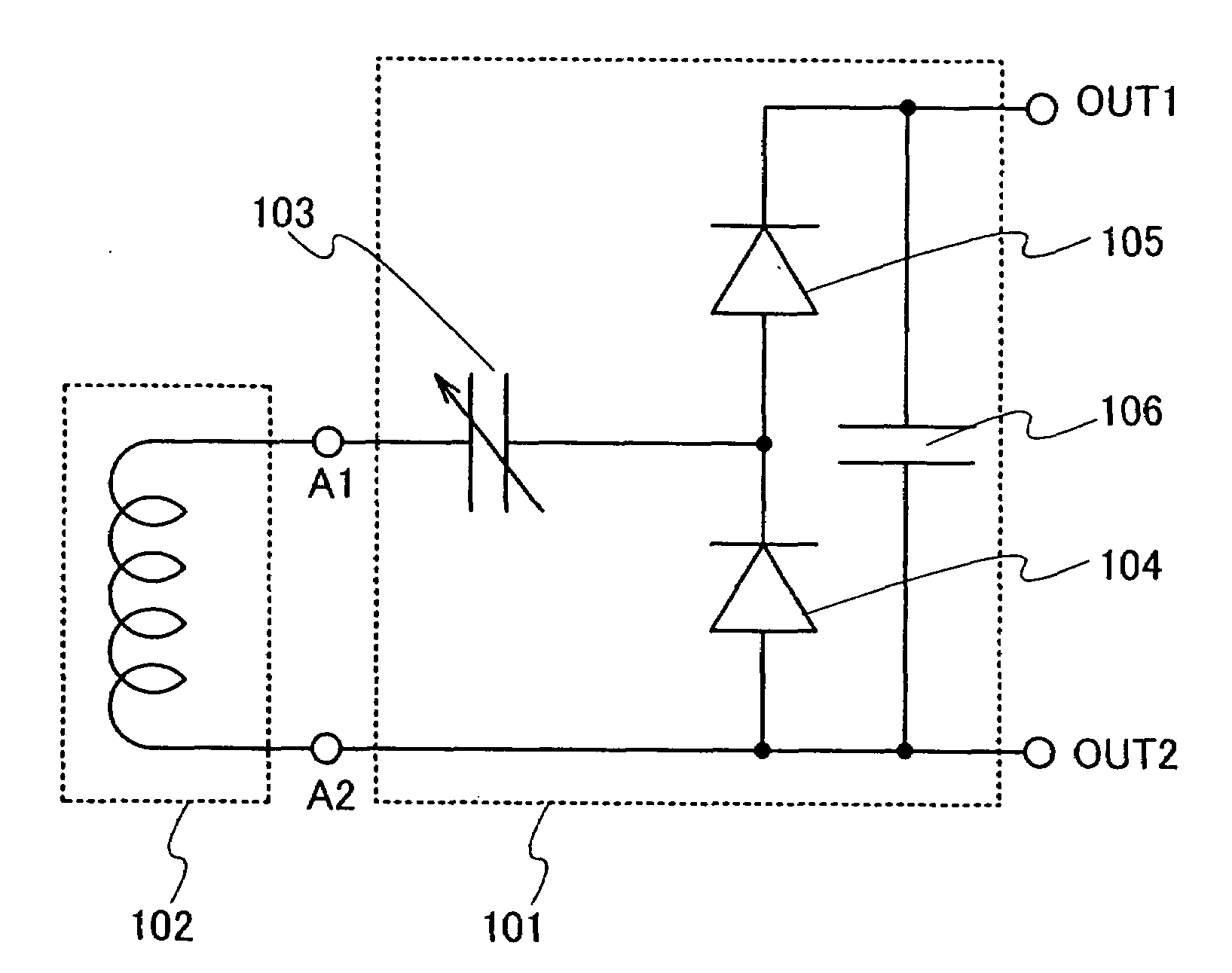
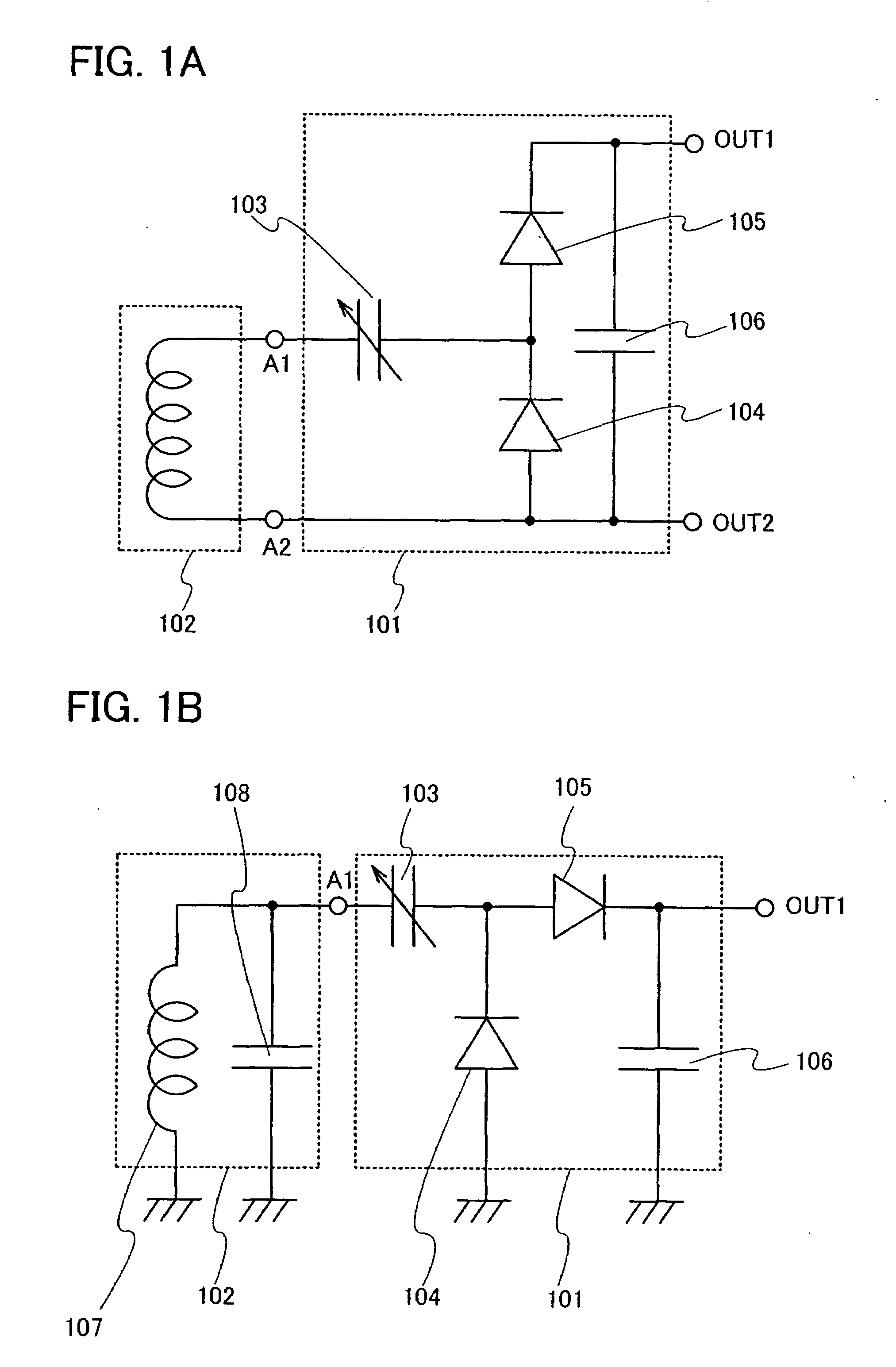
[0048]A structure of a rectifier circuit of the present invention is described with reference to FIGS. 1A and 1B. In FIG. 1A, a rectifier circuit 101 is connected to a terminal A1 and a terminal A2 of an antenna 102, and the terminal A1 and the terminal A2 of the antenna 102 function as input terminals of the rectifier circuit 101. Note that FIG. 1A shows a case where the antenna 102 has a coil shape; however, the shape of the antenna used in the present invention is not limited to this. When communication is performed using an electric field instead of a magnetic field, the antenna 102 does not necessarily have a coil shape.
[0049]The rectifier circuit 101 includes a variable capacitor 103, a diode 104 and a diode 105 which are for rectifying an AC voltage applied between the terminal A1 and the terminal A2, and a smoothing capacitor 106 for smoothing the rectified voltage. The variable capacitor 103 has at least two electrodes. The capacitance value of the variable capacitor 103 ch...
embodiment mode 2
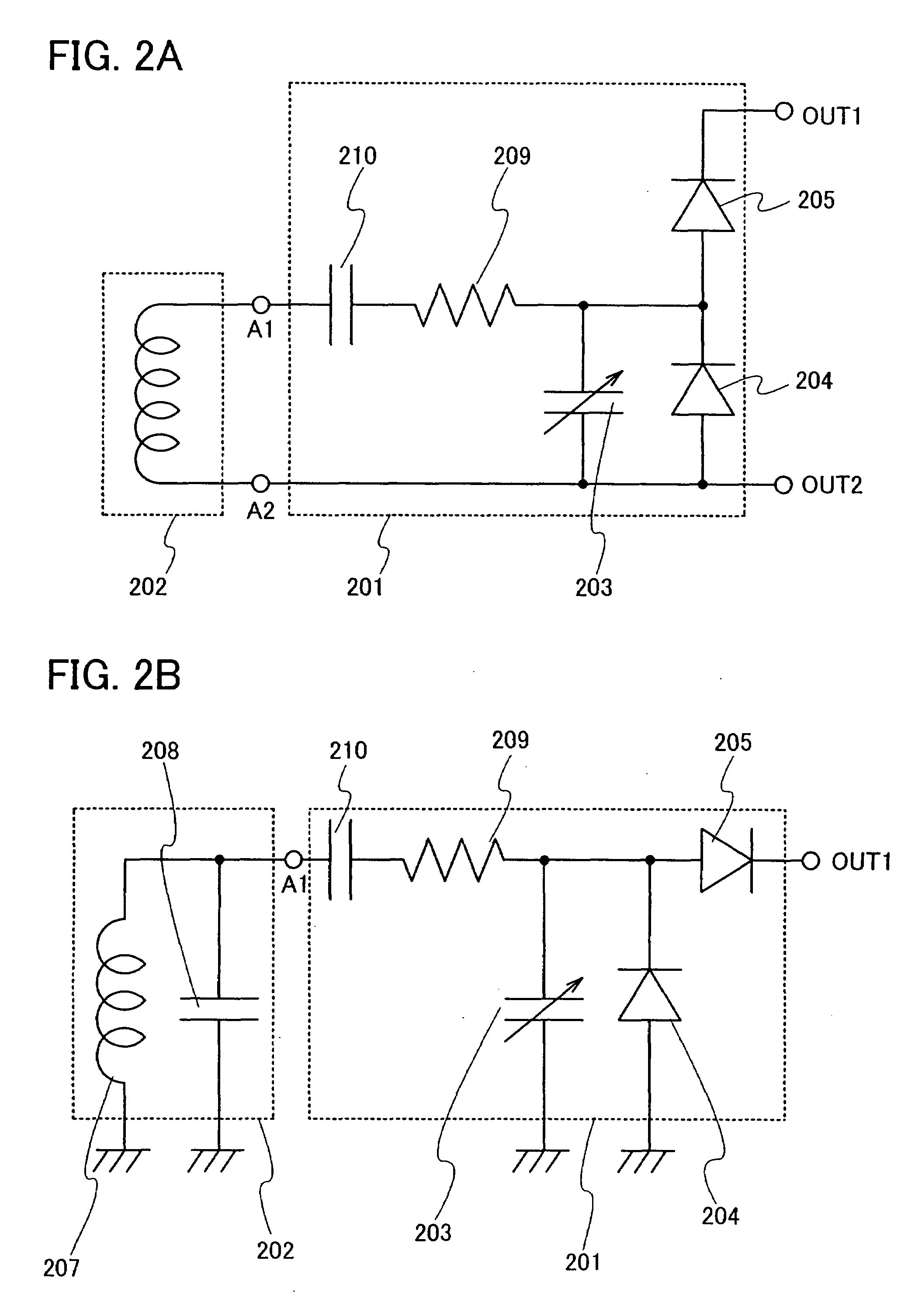
[0067]A structure of the rectifier circuit of the present invention is described with reference to FIGS. 2A and 2B. In FIG. 2A, a rectifier circuit 201 is connected to a terminal A1 and a terminal A2 of an antenna 202, and the terminal A1 and the terminal A2 of the antenna 202 function as input terminals of the rectifier circuit 201. Note that FIG. 2A shows a case where the antenna 202 has a coil shape; however, the shape of the antenna used in the present invention is not limited to this. When communication is performed using an electric field instead of a magnetic field, the antenna 202 does not necessarily have a coil shape.
[0068]The rectifier circuit 201 includes a variable capacitor 203, a diode 204 and a diode 205 which are for rectifying an AC voltage applied between the terminal A1 and the terminal A2, a resistor 209 functioning as a low-pass filter, and a capacitor 210 for making a voltage output from the rectifier circuit twice as high as the voltage. The variable capacito...
embodiment mode 3
[0082]In this embodiment mode, a structure of a rectifier circuit using a MOS (Metal-Oxide Semiconductor) varactor as a variable capacitor is described.
[0083]FIG. 3A shows one mode of the rectifier circuit using a MOS varactor of the present invention. FIG. 3A shows an example in which a MOS varactor is used as the variable capacitor 103 included in the rectifier circuit 101 shown in FIG. 1A. In addition, FIG. 3A shows an example in which MOS transistors are used as the diode 104 and the diode 105.
[0084]A MOS varactor used as the variable capacitor 103 is a p-channel MOS transistor in which a source region (S) and a drain region (D) are electrically connected. A gate electrode (G) of the MOS transistor corresponds to a first electrode of the variable capacitor 103. In addition, the source region (S) and the drain region (D) collectively correspond to a second electrode of the variable capacitor 103.
[0085]A transistor used as the diode 104 is an n-channel MOS transistor in which a so...
PUM
 Abstract
Description
Claims
Application Information