Nonvolatile semiconductor memory device and a method of word lines thereof
a nonvolatile semiconductor and memory device technology, applied in static storage, digital storage, instruments, etc., can solve the problem of difficult shrinkage of tunnel oxide film thickness
- Summary
- Abstract
- Description
- Claims
- Application Information
AI Technical Summary
Benefits of technology
Problems solved by technology
Method used
Image

Examples
embodiment 1
[0059] This embodiment explains the example which performs a different program operation from above-mentioned embodiment in the non-volatile semiconductor memory device of this invention.
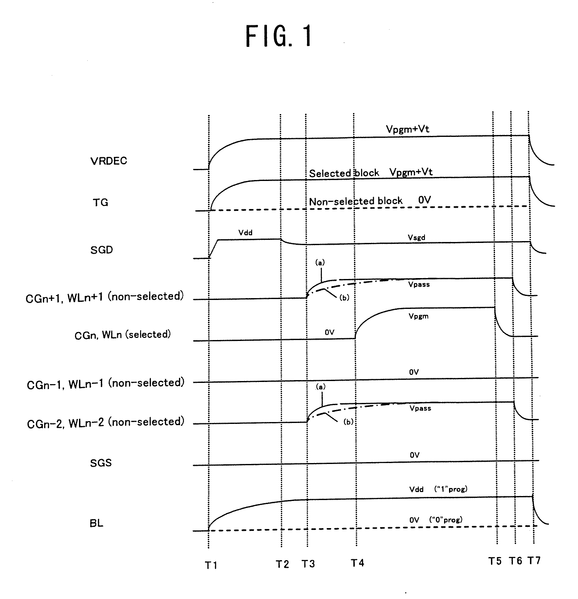
[0060]FIG. 10 is referred to. FIG. 10 is a timing chart in the program operation of the non-volatile semiconductor memory device of this embodiment. In this timing chart, the word line of a selected word line of WLn and others is a non-selected word line. In the time chart of FIG. 10, like the timing chart of FIG. 8, a selected word line is WLn and non-selected word lines are WLn+1, WLn−1, and WLn−2. The word line drive lines corresponding to these word lines are CGn, CGn+1, CGn−1, and CGn−2. In the non-volatile semiconductor memory device of this embodiment, the program operation to timing T5 is the same as that of operation explained in above-mentioned embodiment and above-mentioned FIG. 8. Therefore, the explanation is omitted.
[0061] In this embodiment, program voltage Vpgm of the selected word...
embodiment 2
[0064] This embodiment explains the example which performs a program operation which is different in the above-mentioned embodiment 1 and 2 in the non-volatile semiconductor memory device of this invention.
[0065]FIG. 11 is referred to. FIG. 11 is a timing chart in the program operation of the non-volatile semiconductor memory device of this embodiment. In this timing chart, a selected word line is WLn and other word lines are non-selected word lines. In the time chart of FIG. 11, like the timing chart of FIG. 8, a selected word line is WLn and non-selected word lines are WLn+1, WLn−1, and WLn−2. The word line drive lines corresponding to these word lines are CGn, CGn+1, CGn−1, and CGn−2. In the non-volatile semiconductor memory device of this embodiment, the program operation to timing T5 is the same as that of operation explained in above-mentioned embodiment and above-mentioned FIG. 8. Therefore, the explanation is omitted.
[0066] When discharging program voltage Vpgm of the sele...
PUM
 Abstract
Description
Claims
Application Information
 - Generate Ideas
- Intellectual Property
- Life Sciences
- Materials
- Tech Scout
- Unparalleled Data Quality
- Higher Quality Content
- 60% Fewer Hallucinations
Browse by: Latest US Patents, China's latest patents, Technical Efficacy Thesaurus, Application Domain, Technology Topic, Popular Technical Reports.
© 2025 PatSnap. All rights reserved.Legal|Privacy policy|Modern Slavery Act Transparency Statement|Sitemap|About US| Contact US: help@patsnap.com