High power diode laser having multiple emitters and method for its production

a laser and high-power technology, applied in the field of high-power diode lasers, can solve the problems of high asymmetry of beam quality of such a high-power laser diode, insufficient symmetry of collimated output laser beams in many applications, and more severe asymmetry of beam quality in fast and slow axes. achieve the effect of simple and cost-efficient configuration, low cost and high power

Inactive Publication Date: 2008-04-10
FRAUNHOFER USA
View PDF6 Cites 49 Cited by
  • Summary
  • Abstract
  • Description
  • Claims
  • Application Information

AI Technical Summary

Benefits of technology

[0014] It is an object of the present invention to provide a high power laser diode having a simple and cost-efficient configuration enabling a minimum amount and less tight tolerances of down-stream optics used for collimating output laser beams of the laser diode. It is a further related object of the present invention to provide a high power laser diode having a simple and cost-efficient configuration enabling assembly of the laser diode in a precise and cost-efficient manner. It is a further object of the present invention to provide a high power laser diode posing less demanding requirements with regard to heat dissipation. According to a further aspect of the present invention corresponding methods for manufacturing the above high power laser diode are to be provided.

Problems solved by technology

However, it is noted that the beam quality of such a high power laser diode is highly asymmetric.
The issue of asymmetric beam quality in fast and slow axis is much more severe for high power arrays, with multiple single chips arranged in one semiconductor next to each other in slow axis direction.
Nevertheless, the symmetry of said collimated output laser beams is not satisfactory for many applications.
This approach usually requires precise alignment of an array of multiple micro-optical lenses in six axes, which makes the whole setup relatively complex and expensive.
Nevertheless, a substantial loss of beam quality is experienced because of unavoidable tolerances in the parts, such as smile of the lens or diode array, as well as in the alignment of the laser light emitter(s) to the associated optical component(s).
The high effort for precision alignment of the single chip or the respective optics and the associated costs prohibit further exploration.
The tolerances caused by machining the stepped profile and the recesses are too high for precise fast axis collimation.

Method used


Image

  • High power diode laser having multiple emitters and method for its production
  • High power diode laser having multiple emitters and method for its production
  • High power diode laser having multiple emitters and method for its production

Examples


first embodiment

[0047] With reference to FIG. 1a to 6b the configuration of a high power diode laser according to the present invention and the most important steps for manufacturing such a high power diode laser will be described in more detail.

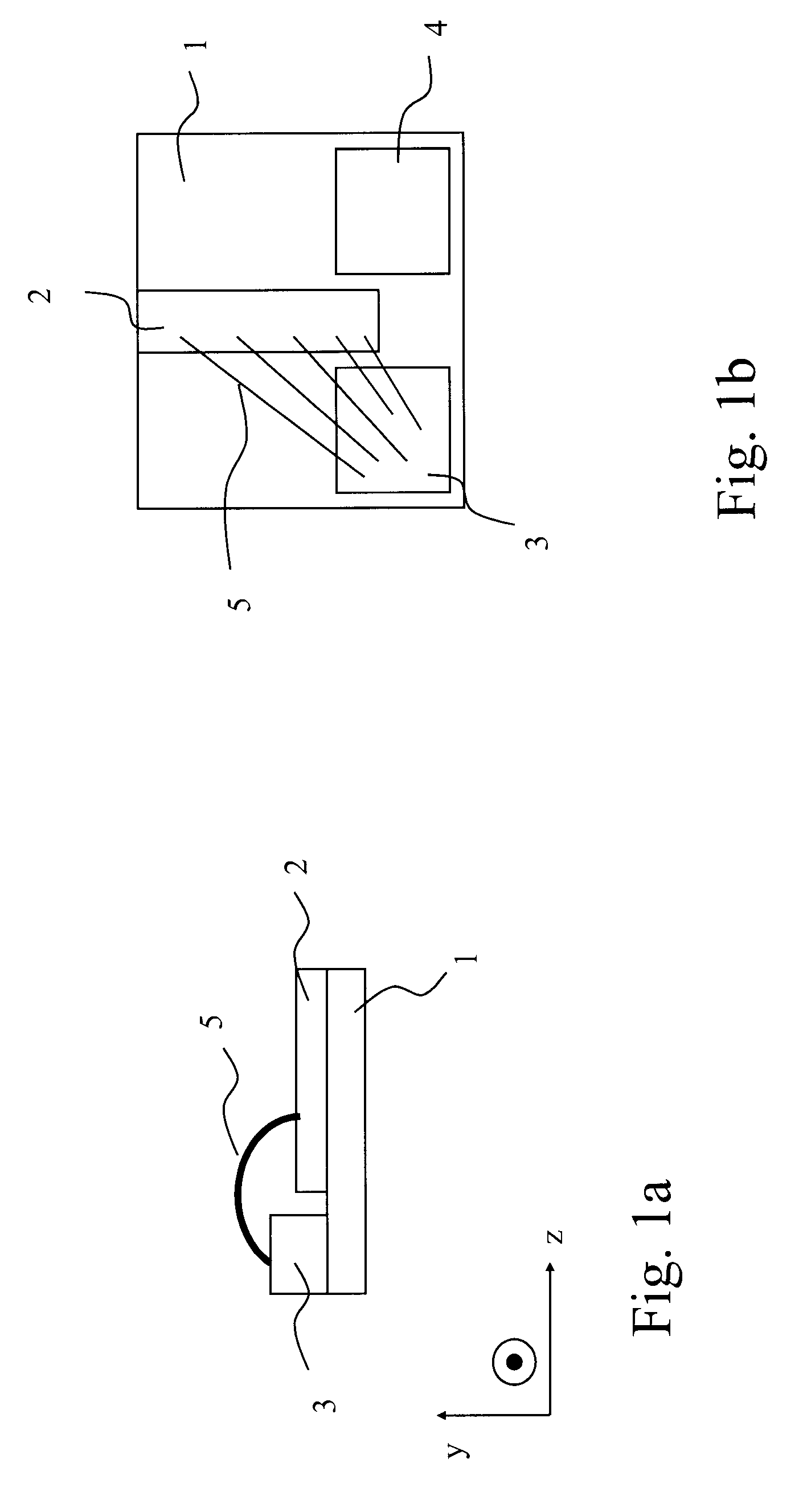
[0048] As shown in FIGS. 1a and 1b, the diode laser chip 2 is mounted on the top surface of a submount 1, which is of a substantially rectangular shape having straight edges perpendicular to each other. The submount 1 can be made of any material suitable for supporting a laser diode chip and preferably has a good heat conductivity in order to spread heat generated by the diode laser chip 2 to a carrier supporting the submount 1. Furthermore, the material of the submount 1 preferably has the same coefficient of thermal expansion as the semiconductor material of the diode laser chip. Suitable materials for the submount 1 that shall not be deemed limiting the present invention are: AlN, CuWo or diamond. Typical dimensions of a submount 1 for use according to t...

second embodiment

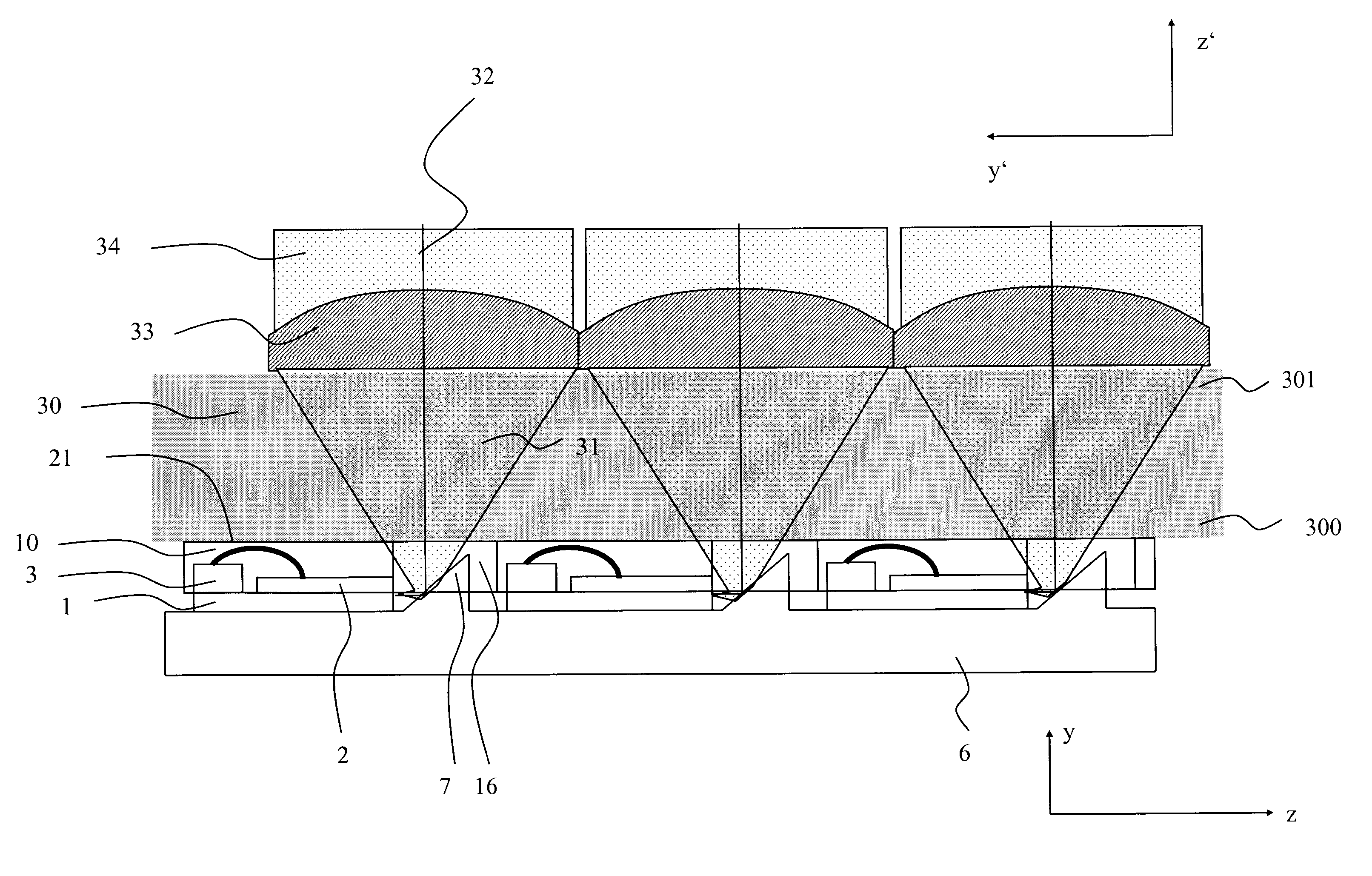
[0067] Referring to FIG. 9 and FIG. 10, a second embodiment according to the present invention will be described. As shown in FIG. 9, the heat sink 6 itself is provided with a plurality of rectangular protrusions 25 that are disposed at equidistant spacings in the fast axis direction y. Such heatsinks can be manufactured precisely, e.g. using micro-machining. While the side surfaces 26 of the protrusions 25 form alignment stops for aligning the submounts 1, the upper surfaces 27 serve as abutment surfaces for aligning the spacer substrate 30 in parallel with the bottom of heatsink 6, i.e. perpendicular to the direction of beam propagation (z) of the output laser beams 31. For properly adjusting the position of the submounts 1 in the direction of beam propagation (z) and in the slow axis direction, i.e. perpendicular to the line of drawing of FIG. 9, additional stops (not shown) can be formed on the side surface 26 and / or on the bottom of submount 1. After bonding the submounts 1 to ...


PUM


Abstract

The invention discloses a high power laser diode comprising a plurality of laser light emitters (2) and a plurality of light collimating means (33), wherein each of the laser light emitters (2) defines, in a direction perpendicular to a direction of propagation (32) of an output laser beam, a fast axis (y) and a slow axis (x), and wherein each of the light collimating means is associated with a laser light emitter and configured for collimating the output laser beam at least in a fast axis (y) direction. In order to enable a simple and cost-efficient assembly of the diode laser with collimating means, having a layered structure consisting of a plurality of plane-parallel substrates. For this purpose, the diode laser comprises planar substrate means (10, 30) which serves to precisely define a distance between a respective laser light emitter (2) and an associated light collimating means to the order of one or several millimetres and to support the collimating means (33) such that the optical axis of said laser light emitters are parallel to each other and for defining a precise location of emitters on the planar substrate (10), preferably at predetermined distance in fast axis direction between said laser light emitters. The collimating means is an array or multiple single of micro-optical lenses having a rear side which is bonded to the upper surface of the planar spacer means. The submounts of the light emitters (2) are mounted to the planar substrate means (10, 30) and to a heatsink (6).

Description

[0001] The present application is related to and claims benefit under 35 U.S.C. §119 of U.S. Provisional Patent Application No. 60 / 778,806, filed on Mar. 3, 2007 with the title ‘High Power Diode Laser Having Multiple Emitters and Method for its Production’ the whole content of which is hereby incorporated by reference.FIELD OF THE INVENTION [0002] The present invention relates in general to high power diode laser and relates in particular to a high power diode laser having multiple emitters and a method for manufacturing the same. BACKGROUND OF THE INVENTION [0003] Most high power diode lasers are edge emitting semiconductors, with the laser emitted from one facet. Typical dimensions of one diode laser are a facet of 500 microns width and 100 microns height with a length between 0.6 mm to 3 mm. The optical brightness of the diode laser is defined by its internal structure. Parallel to the pn-junction (fast axis) the emission is diffraction limited and emerging from an aperture of ab...

Claims


Application Information

Patent Timeline
Patent Type & Authority Applications(United States)
IPC IPC(8): H01S5/00
CPCG02B27/0961H01S5/005H01L2224/48091H01S5/0071H01S5/02248H01S5/02252H01S5/02256H01S5/02276H01S5/02288H01S5/02476H01S5/4012H01S5/4031G02B19/0057G02B19/0014H01L2924/00014H01S5/02355H01S5/02326H01S5/02325H01S5/02345H01S5/02253
Inventor DOERFEL, FALKHEINEMANN, STEFANWITTE, REINER
Owner FRAUNHOFER USA
Why Eureka
Try Eureka