
Use of perylene diimide derivatives as air-stable n-channel organic semiconductors

a technology of organic semiconductors and perylene diimide, which is applied in the direction of thermoelectric devices, naphthalimide/phthalimide dyes, anthracene dyes, etc., can solve the problems of uneconomic use of said materials and does not teach a method for the production of ofets

Inactive Publication Date: 2008-04-17
BASF AG +1
View PDF2 Cites 19 Cited by
  • Summary
  • Abstract
  • Description
  • Claims
  • Application Information

AI Technical Summary

Benefits of technology

[0059]The method according to the invention can be used to provide a wide variety of devices. Such devices may include electrical devices, optical devices, optoelectronic devices (e.g. semiconductor devices for communications and other applications such as light emitting diodes, electroabsorptive modulators and lasers), mechanical devices and combinations thereof. Functional devices assembled from transistors obtained according to the method of the present invention may be used to produce various IC architectures. Further, at least one compound of the formula (I) may be employed in conventional semiconductor devices, such as diodes, light-emitting diodes (LEDs), inverters, sensors, and bipolar transistors. One aspect of the present invention includes the use of the method of the invention to fabricate an electronic device from adjacent n-type and / or p-type semiconducting components. This includes any device that can be made by the method of the invention that one of ordinary skill in the art would desirably make using semiconductors. Examples of such devices include, but are not limited to, field effect transistors (FETs), bipolar junction transistors (BJTs), tunnel diodes, modulation doped superlattices, complementary inverters, light-emitting devices, light-sensing devices, biological system imagers, biological and chemical detectors or sensors, thermal or temperature detectors, Josephine junctions, nanoscale light sources, photodetectors such as polarization-sensitive photodetectors, gates, inverters, AND, NAND, NOT, OR, TOR, and NOR gates, latches, flip-flops, registers, switches, clock circuitry, static or dynamic memory devices and arrays, state machines, gate arrays, and any other dynamic or sequential logic or other digital devices including programmable circuits.

Problems solved by technology

However, this usually requires a complicated synthesis which makes the use of said materials uneconomic.
This document also does not teach a method for the production of OFETs.

Method used


Image

  • Use of perylene diimide derivatives as air-stable n-channel organic semiconductors
  • Use of perylene diimide derivatives as air-stable n-channel organic semiconductors
  • Use of perylene diimide derivatives as air-stable n-channel organic semiconductors

Examples


examples

[0149]I) BPE-PTCDI

[0150]BPE-PTCDI was synthesized form peryiene-3,4:9,10-tetracarboxylic acid bisanhydride and phenethylamine by known methods. The purification was carried out by three consecutive vacuum sublimations using a three-temperature-zone furnace (Lindberg / Blue Thermo Electron Corporation). The three temperature zones were set to be: 400° C., 350° C. and 300° C. and the vacuum level during sublimation was 10−6 Torr or less while the starting material was placed in the first temperature zone.

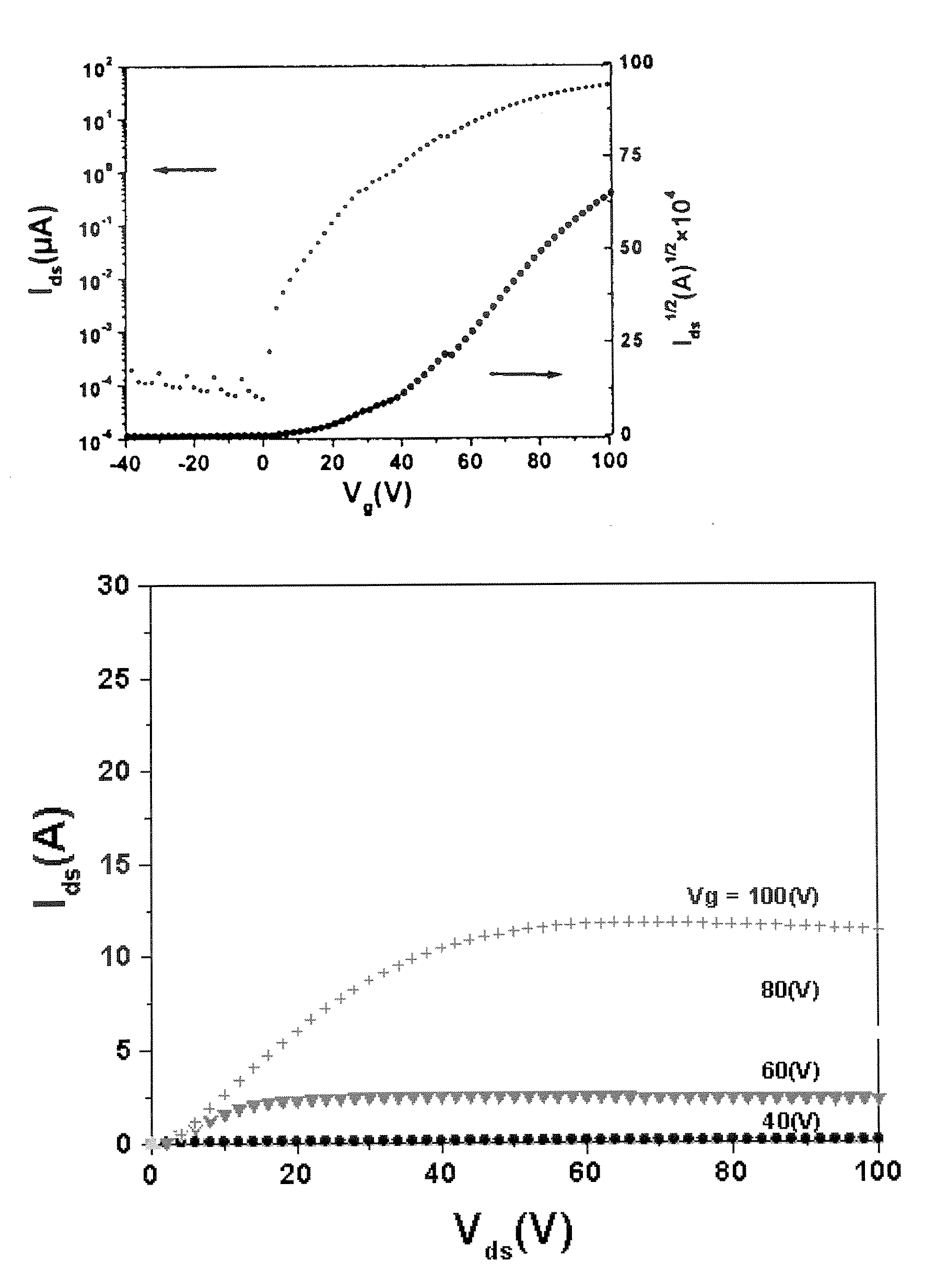
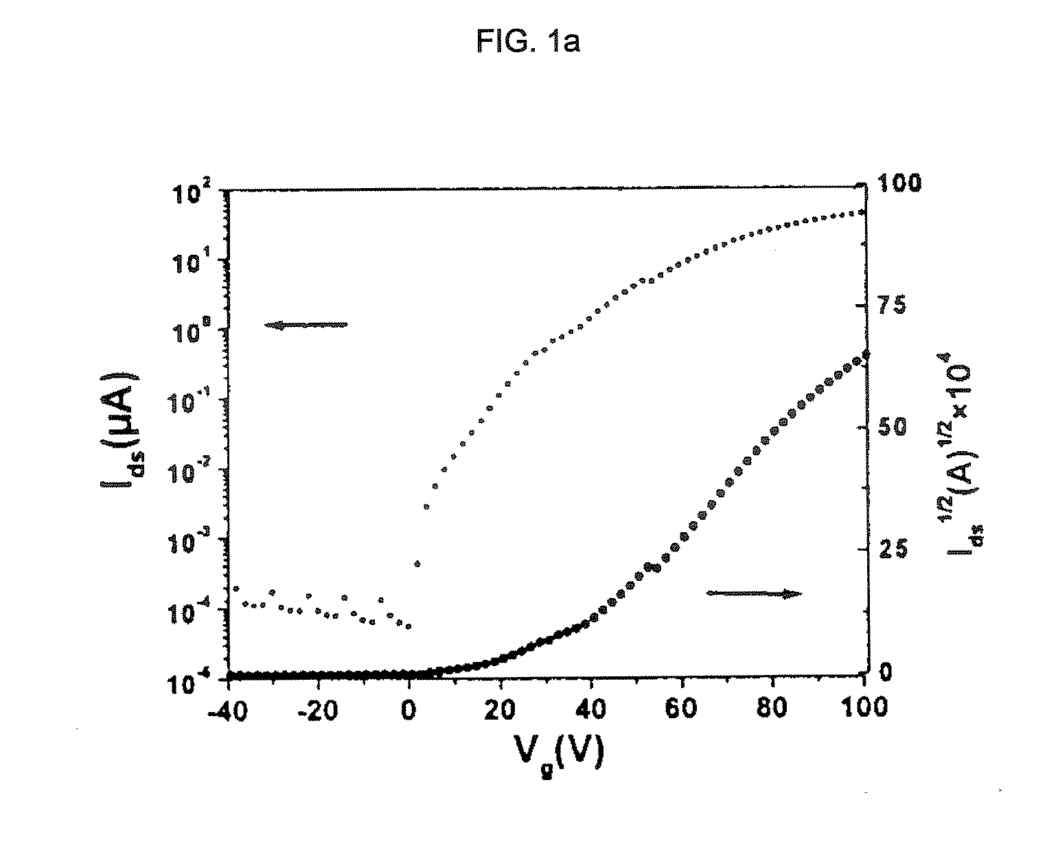
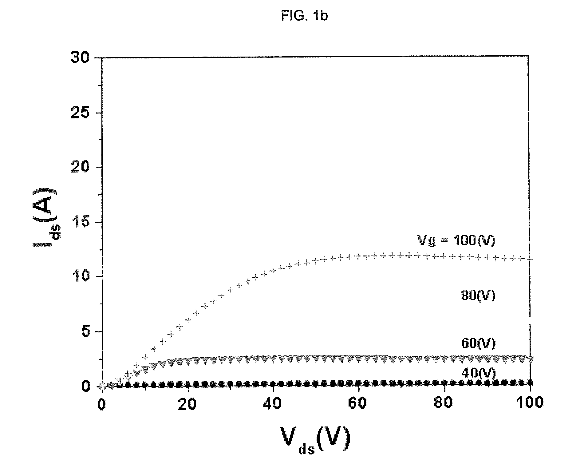
[0151]Highly doped n-type Si wafers (2.5×2.5 cm) with a thermally grown dry oxide layer (capacitance per unit area Ci=10 nF / cm2) as gate dielectric were used as substrates. The substrate surfaces were cleaned with acetone followed by isopropanol. Afterwards, the surface of the substrate was left unmodified (a) or was modified with n-octadecyl trimethoxysilane (b) or hexamethyidisilazane (c):[0152](a) No surface treatment[0153](b) A few drops of n-octadecyl trimethoxysilane (C18H37Si(OCH...


PUM

PropertyMeasurementUnit
temperatureaaaaaaaaaa
thicknessaaaaaaaaaa

Abstract

The present invention relates to the use of of perylene diimide derivatives as air-stable n-type organic semiconductors.

Description

BACKGROUND OF THE INVENTION[0001]1. Field of the Invention[0002]The present invention relates to the use of perylene diimide derivatives as air-stable n-type organic semiconductors.[0003]2. Description of the Related Art[0004]In the field of microelectronics there is a constant need to develop smaller device elements that can be reproduced conveniently and inexpensively at a lowest possible failure rate. Modern digital integrated circuits are based on field-effect transistors (FET), which rely on an electric field to control the conductivity of a “channel” in a semiconductor material. Organic field-effect transistors (OFET) allow the production of flexible or unbreakable substrates for integrated circuits having large active areas. As OFETs enable the production of complex circuits, they have a wide area of potential application (e.g. in driver circuits of pixel displays). A thin film transistor (TFT) is a special kind of field effect transistor made by depositing thin films for the...

Claims


Application Information

Patent Timeline
Patent Type & Authority Applications(United States)
IPC IPC(8): H01L29/08C07D471/02H01L51/40
CPCC07D471/06H01L51/001Y02E10/549H01L51/0545H01L51/0053C09B5/62C09B57/08
Inventor KOENEMANN, MARTINERK, PETERGOMEZ, MARCOSBAO, ZHENAN
Owner BASF AG
Learn More