

Electro-optical device and electronic apparatus
a technology of optical devices and electronic devices, applied in the direction of static indicating devices, non-linear optics, instruments, etc., can solve the problems of insufficient light shielding for the peripheral circuit portion, damage to semiconductor elements such as tfts, included in various circuits, etc., and achieve the effect of reducing damage to semiconductor elements
- Summary
- Abstract
- Description
- Claims
- Application Information
AI Technical Summary
Benefits of technology
Problems solved by technology
Method used
Image

Examples
Embodiment Construction
[0029]An electro-optical device and an electronic apparatus according to exemplary embodiments of the invention will be described hereinafter with reference to the drawings.
1: Electro-Optical Device
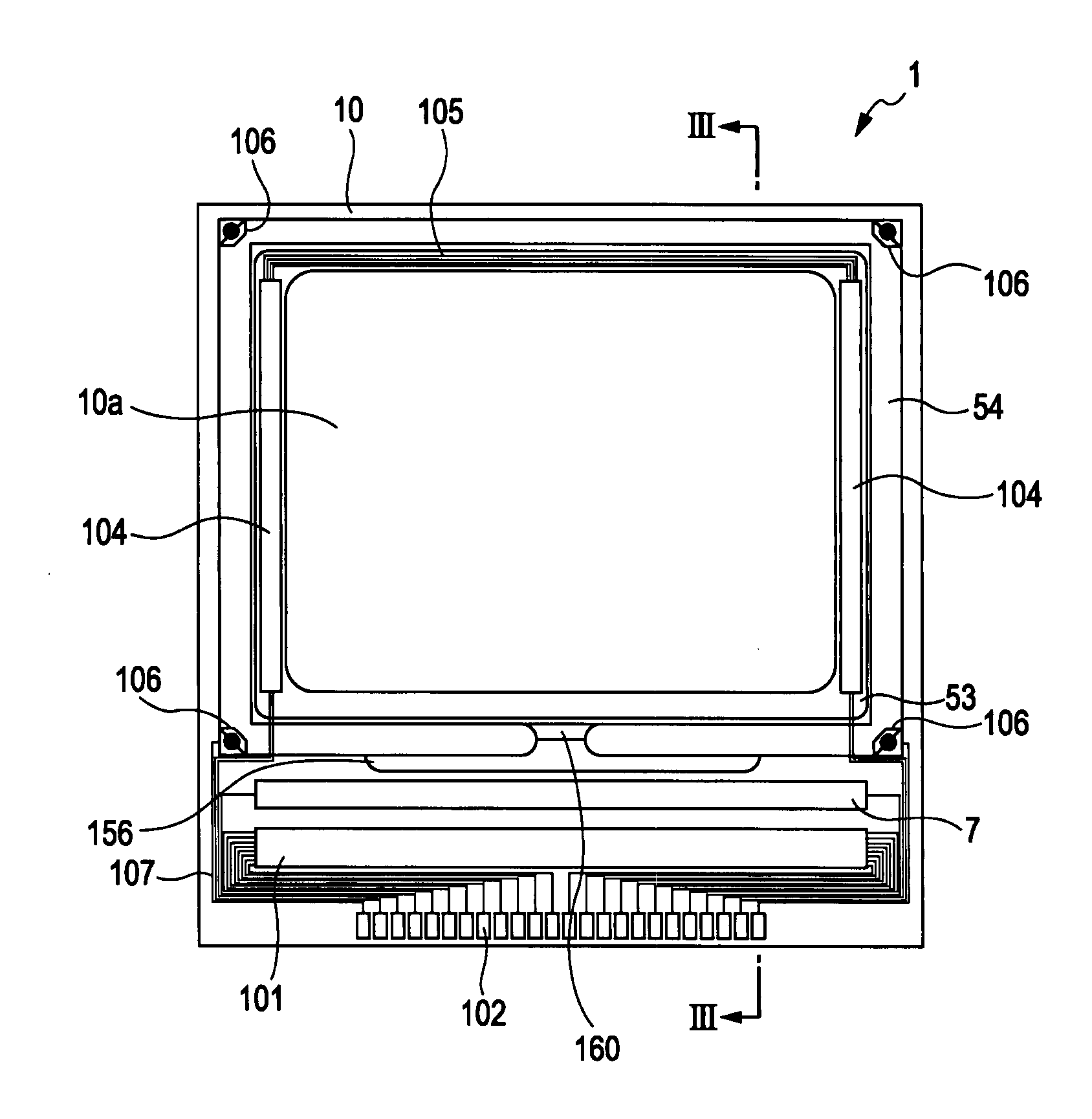
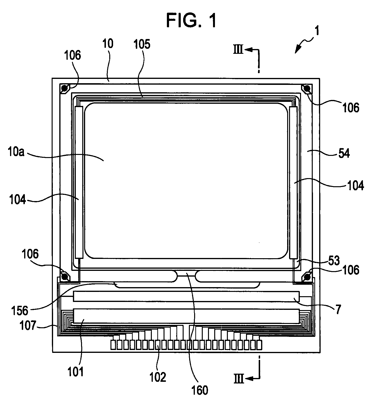
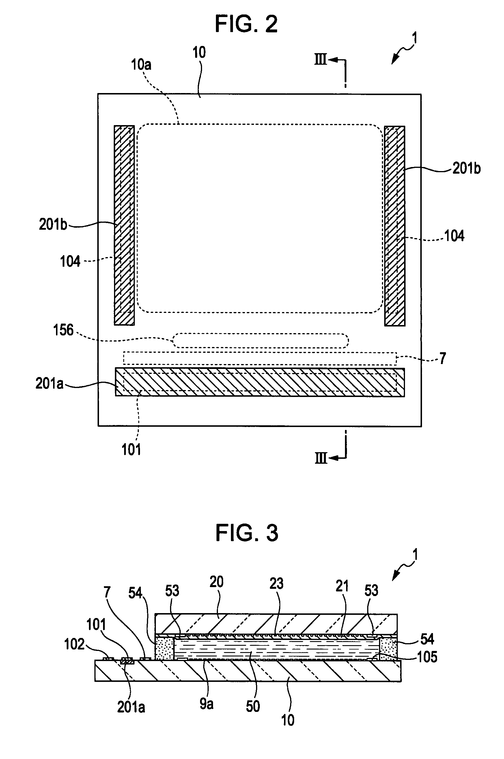
[0030]A specific configuration of an electro-optical device according to an embodiment of the invention will now be described below with reference to FIGS. 1 to 3. In the embodiment, an example of the electro-optical device is discussed below in the context of a liquid crystal device 1 that employs a TFT active matrix display type. FIG. 1 is a plan view illustrating the liquid crystal device 1 when viewed from a counter substrate. FIG. 2 is a plan view illustrating essential portions of the liquid crystal device 1. FIG. 3 is a sectional view taken along the line III-III of each of FIGS. 1 and 2.
[0031]Referring to FIGS. 1 and 3, the liquid crystal device 1 includes a TFT array substrate 10 and a counter substrate 20 that are disposed facing each other. A liquid crystal layer 50 is sealed b...
PUM
 Abstract
Description
Claims
Application Information