Method of forming an integrated optical polarization grid on an LCD subsrate and liquid crystal display manufactured to include the grid

a technology of optical polarization grid and integrated optical polarization, which is applied in the direction of polarizing elements, instruments, photomechanical equipment, etc., can solve the problems that the polarizing characteristics of the polarizer will also be decreased, and the polarizing characteristics of the polarizer cannot be reliably manufactured

Active Publication Date: 2008-05-01
SAMSUNG DISPLAY CO LTD
View PDF7 Cites 48 Cited by
  • Summary
  • Abstract
  • Description
  • Claims
  • Application Information

AI Technical Summary

Problems solved by technology

However, because in this application a metallic reflective film typically needs to be formed by patterning a metallic layer at a nano scale of about 50 nm to 200 nm, such a wire grid polarizer cannot be reliably manufactured if the metal patterning process does not provide sufficient fine resolution and repeatedability during mass production.
In addition, it appears that polarizing characteristics of the polarizer will also be decreased by lack of uniformity in a wire grid polarizing pattern produced by such conventional application of the nano-imprint technique.

Method used


Image

  • Method of forming an integrated optical polarization grid on an LCD subsrate and liquid crystal display manufactured to include the grid
  • Method of forming an integrated optical polarization grid on an LCD subsrate and liquid crystal display manufactured to include the grid
  • Method of forming an integrated optical polarization grid on an LCD subsrate and liquid crystal display manufactured to include the grid

Examples


Embodiment Construction

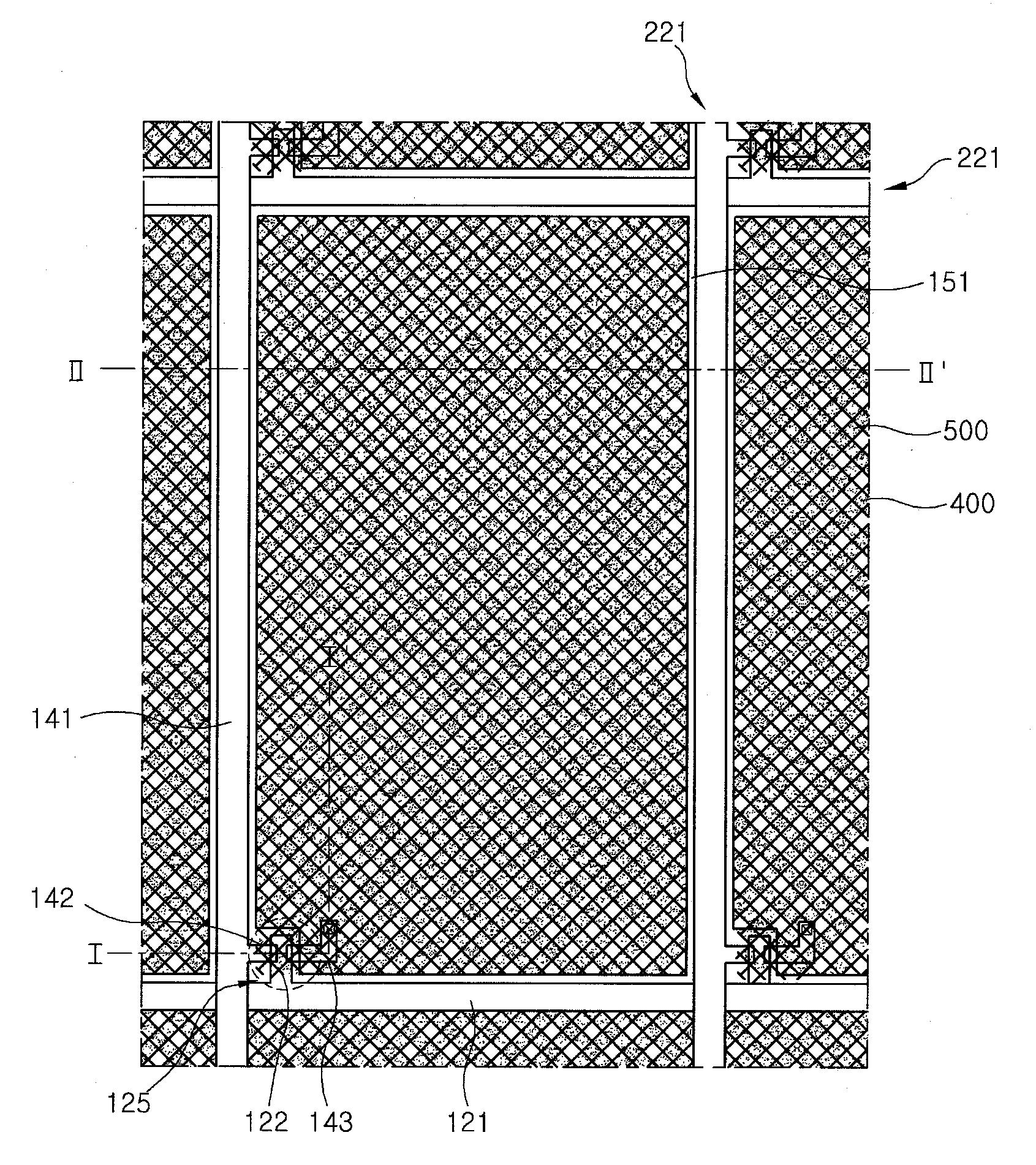
[0028]As for the accompanying drawings, illustrated thicknesses are not necessarily to scale and some were expanded to more clearly show the several layers and regions.

[0029]Same reference numerals are generally used to designate alike or same parts. It will be understood that when an element, such as a layer, film, region, plate, is referred to as being “over” or “on” another element, it not only may be “directly over” or “directly on”, but also it may have another element interposed in between unless it is said to be directly on.

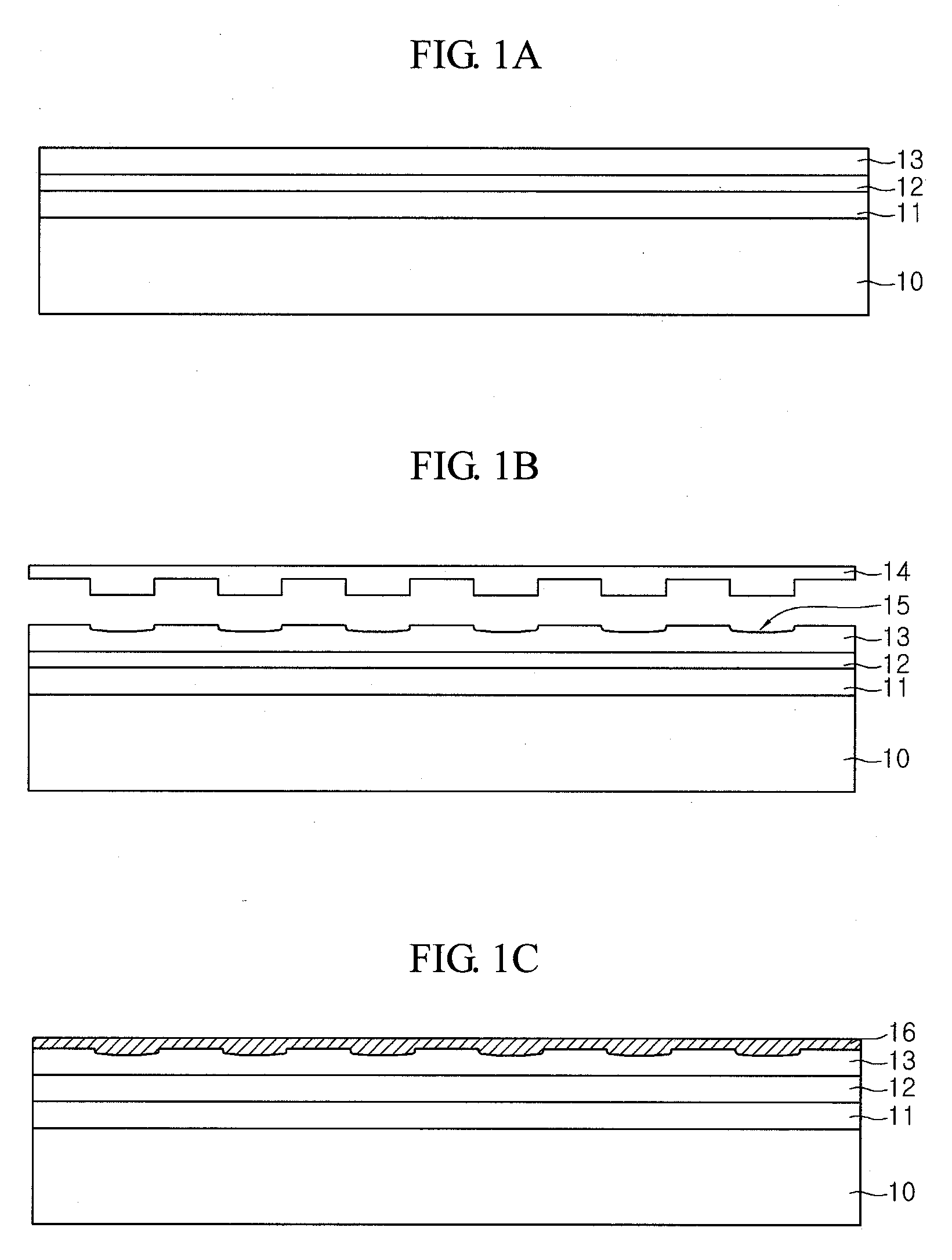
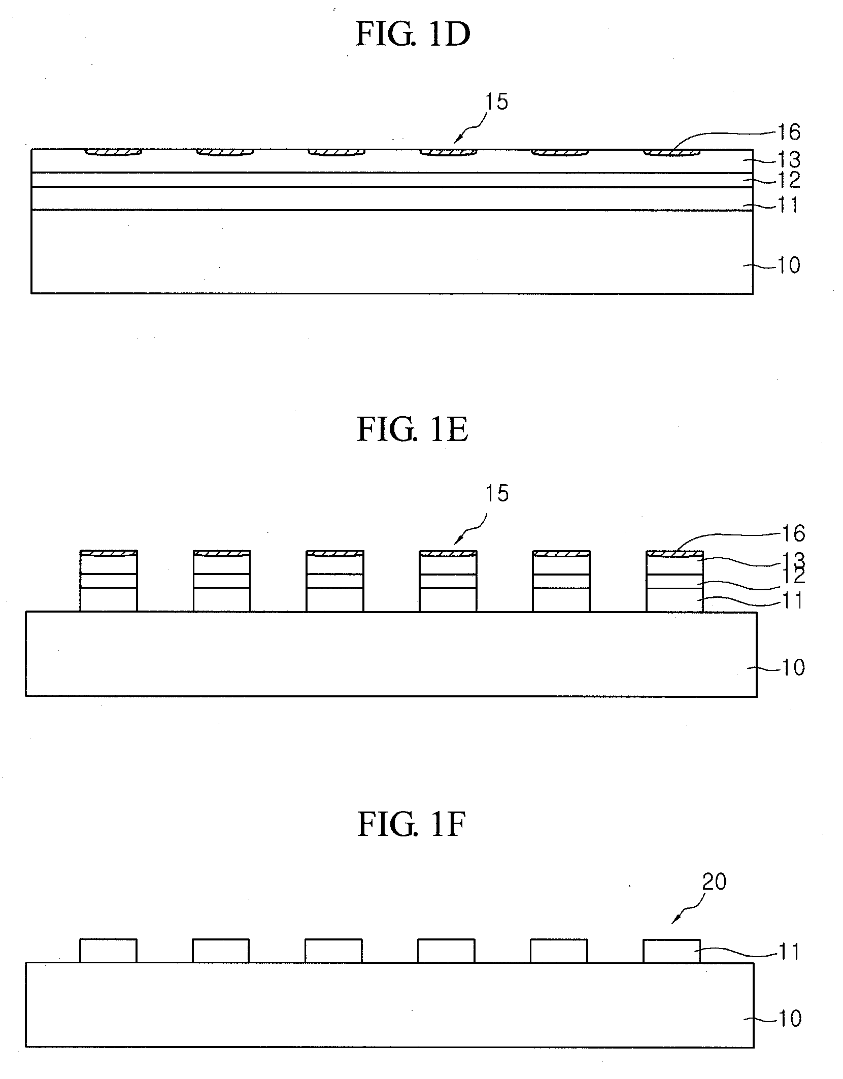
[0030]FIGS. 1A to 1F are cross-sectional views showing sequential processing steps that illustrate a method of forming a wire grid polarizing pattern according to an embodiment of the present disclosure.

[0031]Referring to FIG. 1A, a reflective layer 11, an anti-reflective film 12, and a UV-hardenable and / or heat-hardenable soft film such as a photosensitive polymer film 13 are sequentially formed on a transparent substrate 10 as shown. The substrate 10 may...


PUM

PropertyMeasurementUnit
diameteraaaaaaaaaa
diameteraaaaaaaaaa
thicknessaaaaaaaaaa

Abstract

A method of forming a wire grid polarizing pattern across the relatively large surface area of a display substrate is disclosed where the method includes using a nano imprint lithograph process.
According to the disclosure, in forming the wire grid polarizing patterns using nano imprint lithography process, wire grid polarizing patterns are formed by bonding a stamp having a stamping area substantially smaller than that of the substrate with successive reticle areas of the substrate, where the substrate has a photosensitive film deposited thereon and where the stamping is such that recesses having a predetermined depth are formed in the photosensitive film, and then filling the recesses with an insulating film and etching it using the insulating film as a mask.
Accordingly, since a mechanical misalignment margin is acceptable from one reticle area to the next when patterning across the entire operational surface of the photosensitive film, a wire grid polarizing pattern with a uniform line width and spacings in each reticle area can be formed on a substrate having a large area for use with a liquid crystal panel.

Description

BACKGROUND[0001]1. Field of Invention[0002]The present disclosure of invention relates to a method of forming an optical polarizing grid and to a liquid crystal display having the same, and particularly to a method of integrally forming a metallic polarizing grid by means of applying a nano-scale imprint lithography process to a substrate that has a relatively large surface area such as in the case of liquid crystal display panels.[0003]2. Description of Related Art[0004]A liquid crystal display (LCD) is typically composed of a thin film transistors (TFT) supporting substrate having pixel electrodes formed thereon, and a color filters supporting substrate having a common electrode formed thereon. The typical LCD also has a liquid crystal material layer inserted in between the TFT-supporting and filters-supporting substrates. A liquid crystal display can display images by applying appropriate voltages between the pixel electrodes and the common electrode at respective pixel areas so ...

Claims


Application Information

Patent Timeline
Patent Type & Authority Applications(United States)
IPC IPC(8): B29D11/00G02B5/30G02F1/1335
CPCG02B5/3058B29D11/0074G02F1/1335
Inventor CHOO, DAE HOYU, YEON HEEKIM, HONG GYUN
Owner SAMSUNG DISPLAY CO LTD
Why Eureka
Try Eureka