Light-emitting device

a technology of light-emitting devices and active layers, which is applied in the direction of semiconductor devices, basic electric elements, electrical apparatus, etc., can solve the problems of many displacements, easy to affect the active layer (luminescent layer), and become electrically and mechanically vulnerable, so as to minimize the first electrode, maximize the luminescent area, and stabilize the mounting properties

Active Publication Date: 2008-05-08
XIAMEN SANAN OPTOELECTRONICS CO LTD
View PDF11 Cites 28 Cited by
  • Summary
  • Abstract
  • Description
  • Claims
  • Application Information

AI Technical Summary

Benefits of technology

[0008] In the light-emitting diode with the above-described structure, in order to efficiently emit light, it is important to design the first electrode (n-side electrode) 121 so as to minimize the area (width) thereof and prevent deterioration in electric characteristics in consideration of the structure and constitution (composition and carrier concentration) of each compound semiconductor layer, the relation between the current flow and spreading, and contact resistance. Also, in order to achieve the light-emitting diode with higher luminance, it is important to increase the area of the luminescent layer. In the light-emitting diode having determined outer dimensions, the area of the luminescent layer can be increased by decreasing the area of the first electrode (n-side electrode) 121.

Problems solved by technology

Nitride compound semiconductors known as constituent materials for a blue light-emitting diode and a green light-emitting diode easily cause many displacements due to lattice mismatch because there is no complete substrate in comparison with lattice matching-type compound semiconductors, such as GaAs compound semiconductors and InP compound semiconductors, which can form grown crystal layers having the same crystal lattice constants as those of a substrate.
As a result, the active layer (luminescent layer) is easily affected by defects due to displacements and becomes electrically and mechanically vulnerable.

Method used


Image

  • Light-emitting device
  • Light-emitting device
  • Light-emitting device

Examples


first embodiment

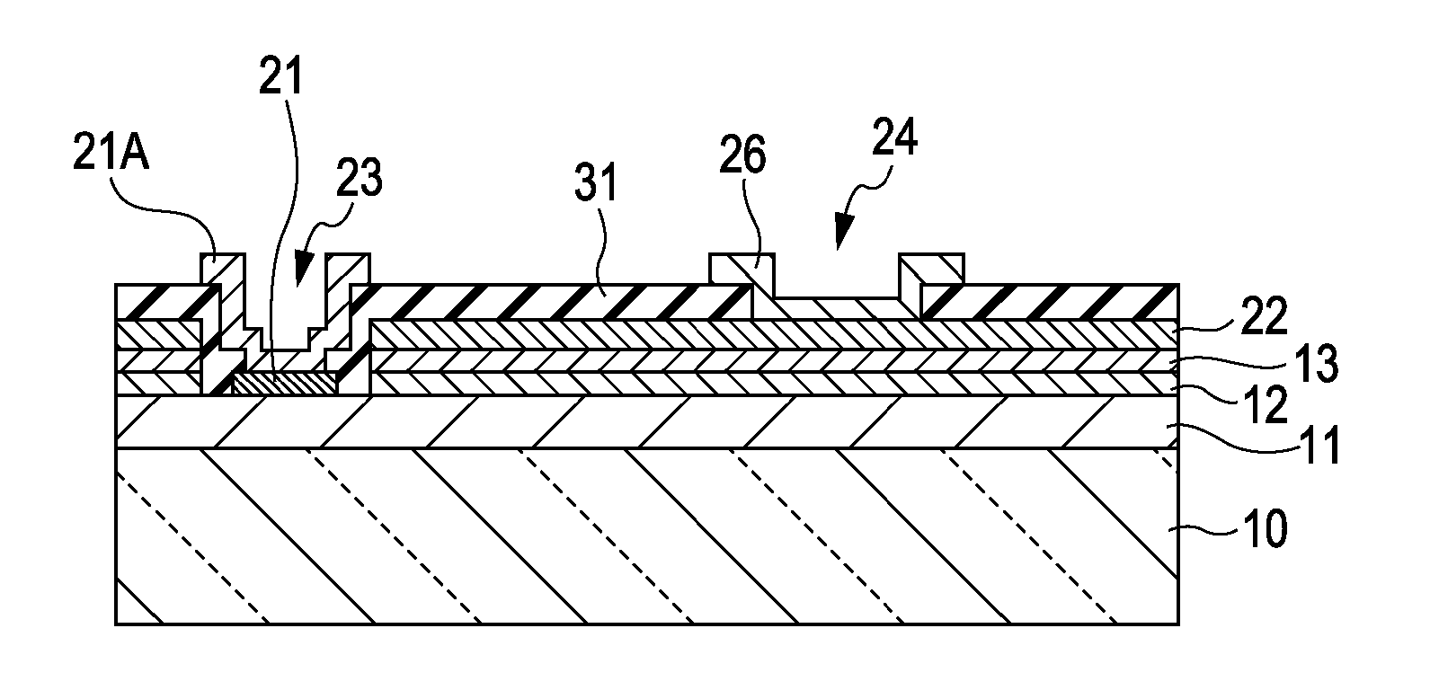
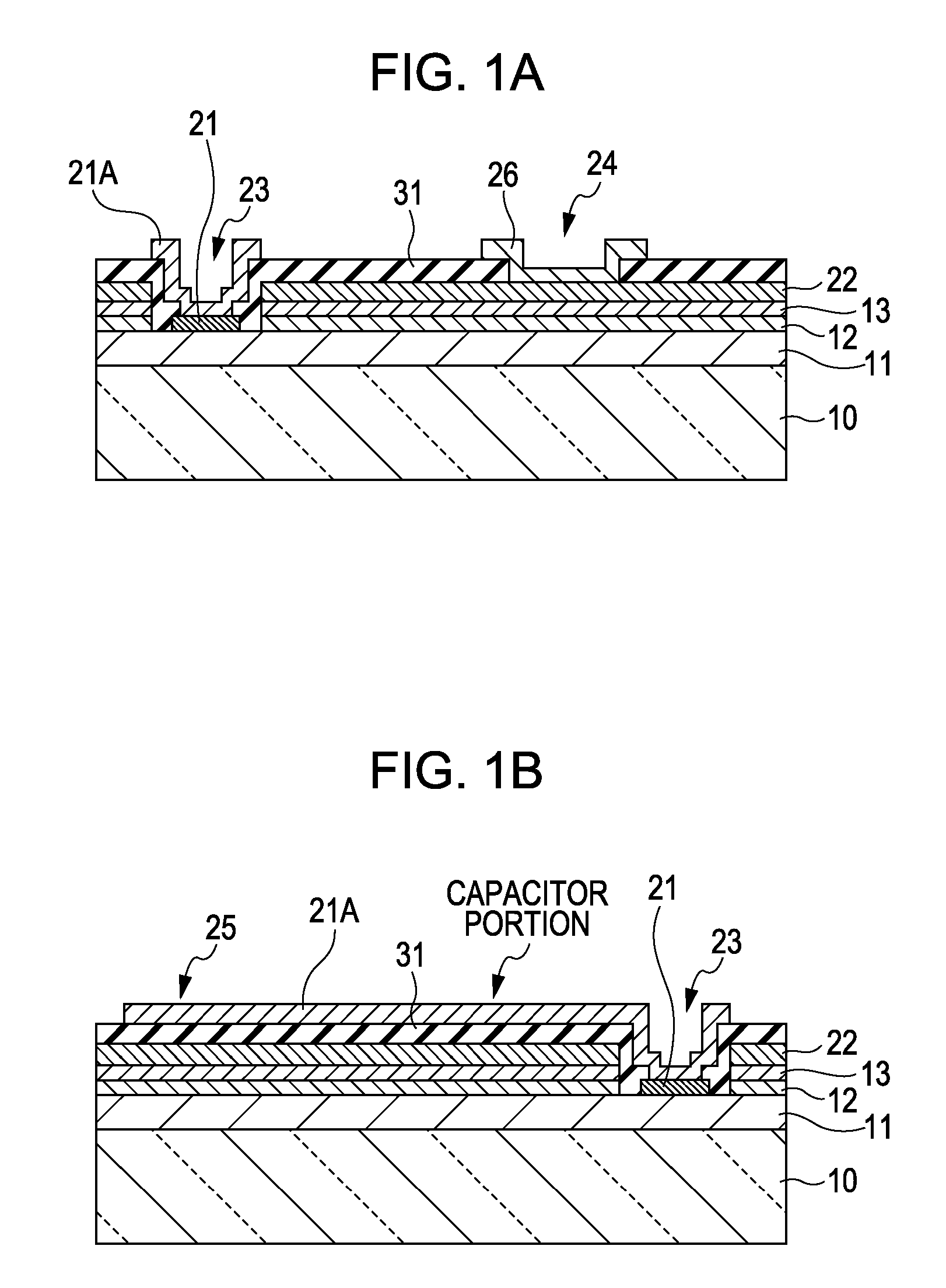
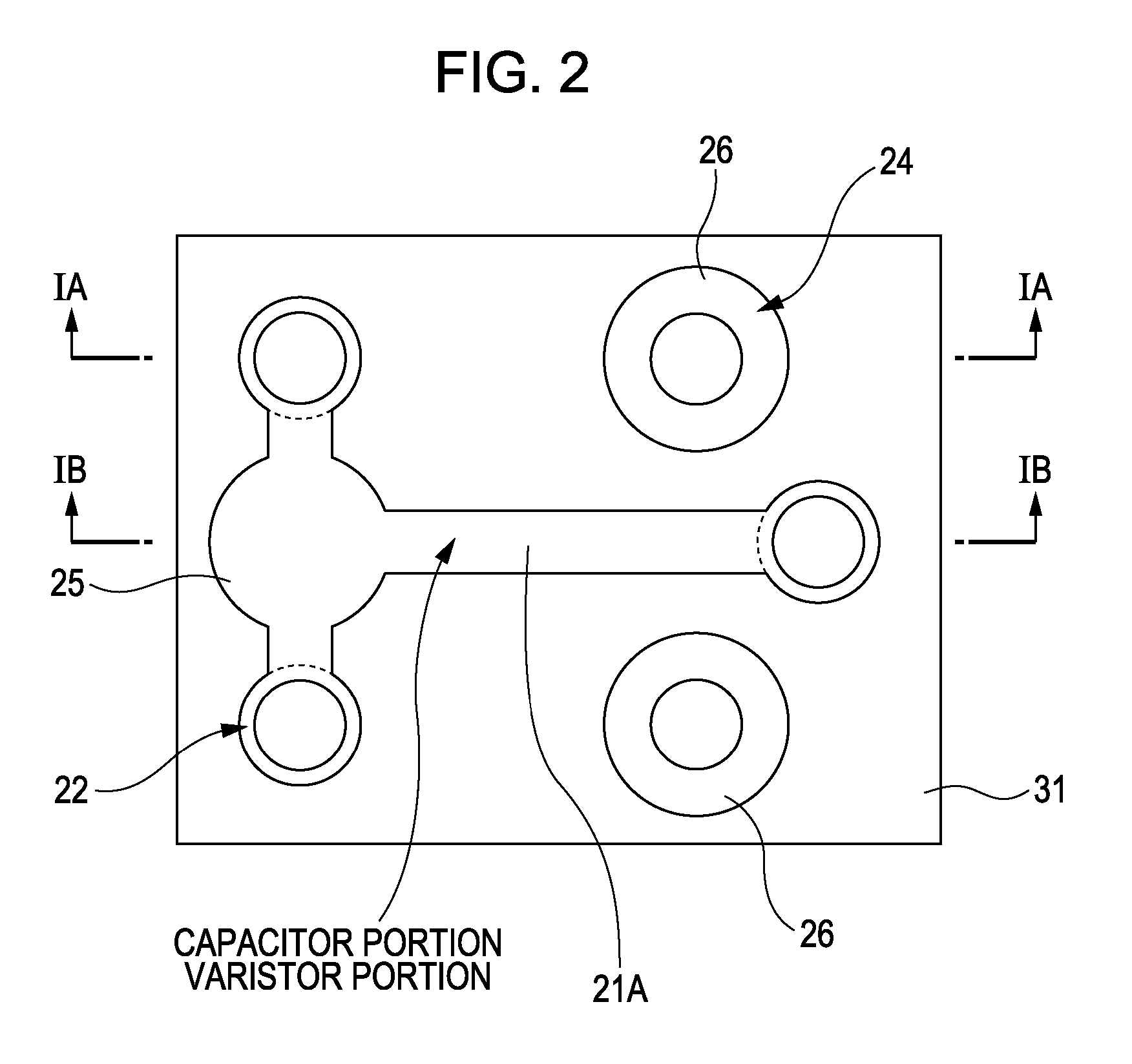
[0053] A first embodiment of the present invention relates to a light-emitting device. The light-emitting device according to the first embodiment includes a light-emitting diode including a GaN compound semiconductor layer. FIG. 2 is a schematic plan view, and FIGS. 1A and 1B are schematic end views taken along arrows IA-IA and IB-IB, respectively, in FIG. 2. As shown in the drawings, the light-emitting device includes the following:

[0054] (A) a first compound semiconductor layer 11 of a first conductivity type (in this embodiment, n-type), an active layer 12 having a quantum well structure, and a second compound semiconductor layer 13 of a second conductivity type (in this embodiment, p-type) different from the first conductivity type;

[0055] (B) a second electrode 22 formed on the second compound semiconductor layer 13 (specifically, over the substantially entire top surface of the second compound semiconductor layer 13);

[0056] (C) an insulating layer 31 covering the second ele...

second embodiment

[0090] The second embodiment is a modification of the first embodiment. In the first embodiment, the insulating layer 31 includes a layer made of the same material. However, in the second embodiment, as shown in FIGS. 8A and 8B which are schematic end views taken along the same arrows as IA-IA and IB-IB in FIG. 2, respectively, the insulating layer includes a first portion 41 provided between a portion of the first electrode extension 21A disposed on the insulating layer and the second electrode 22, and a second portion 42 provided in the other region.

[0091] The first portion 41 of the insulating layer is composed of barium titanate (BaTiO3) like the insulating layer 31 of the first embodiment, while the second portion 42 of the insulating layer is composed of a SOG layer. The first portion 41 of the insulating layer is provided in a portion shadowed in FIG. 2.

[0092] In a usual technique, pinholes or cracks easily occur in an insulating film 114 formed on the basis of the CVD or P...

third embodiment

[0108] The third embodiment is a modification of the second embodiment. In the second embodiment, the first portion 41 of the insulating layer is composed of a barium titanate layer which is a high-dielectric material so that the portion of the first electrode extension 21A which is positioned on the insulating layer, the first portion 41 of the insulating layer, and the second electrode 22 form a capacitor portion. On the other hand, in the third embodiment, as shown in FIGS. 9A and 9B which are schematic end views taken along the same arrows as IA-IA and IB-IB in FIG. 2 and FIG. 12B which is a drawing of an equivalent circuit, a first portion 51 of the insulating layer is composed of a semiconductor ceramic layer, specifically strontium titanate (SrTiO3) so that the portion of the first electrode extension 21A which is positioned on the insulating layer, the first portion 51 of the insulating layer, and the second electrode 22 form a varistor portion.

[0109] Except the above-descr...


PUM


Abstract

A light-emitting device includes a first compound semiconductor layer, an active layer, and a second compound semiconductor layer; a second electrode formed on the second compound semiconductor layer; an insulating layer covering the second electrode; a first opening provided to pass through the insulating layer, the second electrode, the second compound semiconductor layer, and the active layer; a second opening provided to pass through the insulating layer; a first electrode formed on an exposed portion of the first compound semiconductor layer at the bottom of the first opening; a first electrode extension extending from the first electrode to the insulating layer through the first opening and a first pad portion including a portion of the first electrode extension on the insulating layer; and a second pad portion connected to an exposed portion of the second electrode at the bottom of the second opening.

Description

CROSS REFERENCES TO RELATED APPLICATIONS [0001] The present invention contains subject matter related to Japanese Patent Application JP 2006-288422 filed in the Japanese Patent Office on Oct. 24, 2006, the entire contents of which are incorporated herein by reference. BACKGROUND OF THE INVENTION [0002] 1. Field of the Invention [0003] The present invention relates to a light-emitting device. [0004] 2. Description of the Related Art [0005]FIG. 15A is a schematic drawing showing an arrangement of components in a general light-emitting diode (LED) disclosed in, for example, Japanese Utility Model Registration No. 3068914 and FIG. 15B is a schematic sectional view taken along line B-B in FIG. 15A. As shown in FIGS. 15A and 15B, the light-emitting diode includes a substrate 110A made of, for example, sapphire, an underlying layer 110B formed by, for example, a MOCVD method (Metal-Organic Chemical Vapor Deposition) method, and a luminescent layer formed on the substrate 110A and having a ...

Claims


Application Information

Patent Timeline
Patent Type & Authority Applications(United States)
IPC IPC(8): H01L33/00H01L33/06H01L21/28H01L29/417H01L33/38H01L33/44
CPCH01L27/15H01L33/62H01L2924/3011H01L24/45H01L2224/48463H01L2224/45144H01L2924/00014H01L2924/12035H01L2924/12041H01L2224/0603H01L2924/00
Inventor WATANABE, YOSHIAKIHINO, TOMONORIOKANO, NOBUKATAKURAMOCHI, HISAYOSHIOHASHI, TATSUO
Owner XIAMEN SANAN OPTOELECTRONICS CO LTD
Why Eureka
Try Eureka