Method of forming a phase change layer and method of manufacturing a storage node having the phase change layer

a technology of phase change layer and manufacturing method, which is applied in the direction of solid-state devices, coatings, chemical vapor deposition coatings, etc., can solve the problems of difficult control of the growth of the gst layer, and achieve the reduction of the reset current of the pram, the effect of increasing the step coverage and reducing the transistor siz

Inactive Publication Date: 2008-05-08
SAMSUNG ELECTRONICS CO LTD
View PDF6 Cites 37 Cited by
  • Summary
  • Abstract
  • Description
  • Claims
  • Application Information

AI Technical Summary

Benefits of technology

[0012] By forming a phase change (e.g., GST) layer with a CVD or ALD process using a temperature of about 300° C. or lower, increased step coverage may be achieved. Thus, a via hole having a diameter o

Problems solved by technology

However, controlling the growth of the GST la

Method used


Image

  • Method of forming a phase change layer and method of manufacturing a storage node having the phase change layer
  • Method of forming a phase change layer and method of manufacturing a storage node having the phase change layer
  • Method of forming a phase change layer and method of manufacturing a storage node having the phase change layer

Examples


Embodiment Construction

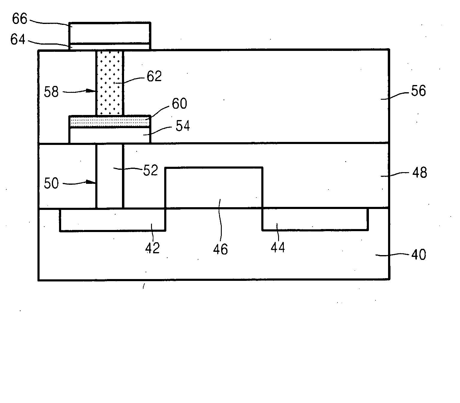
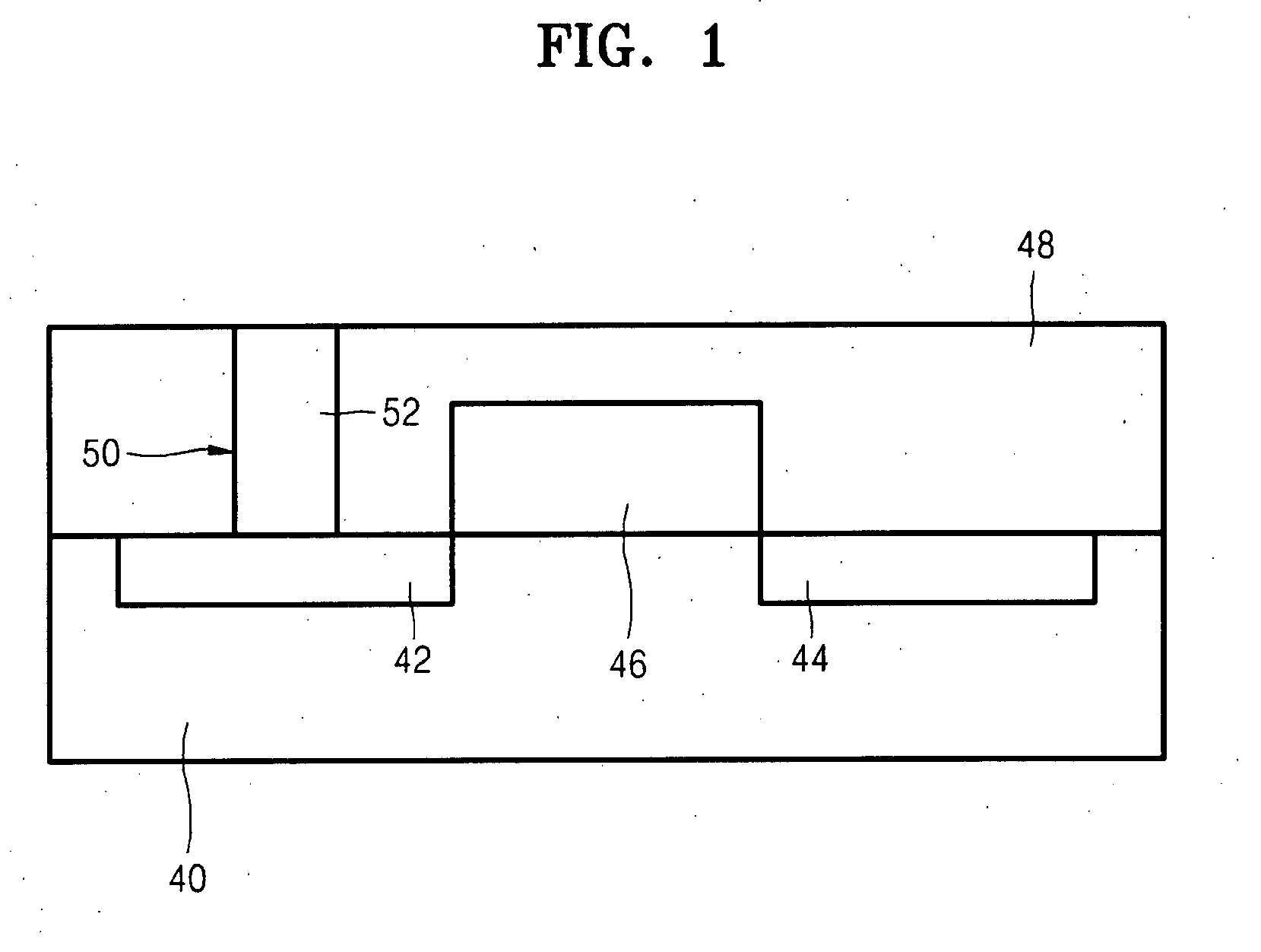
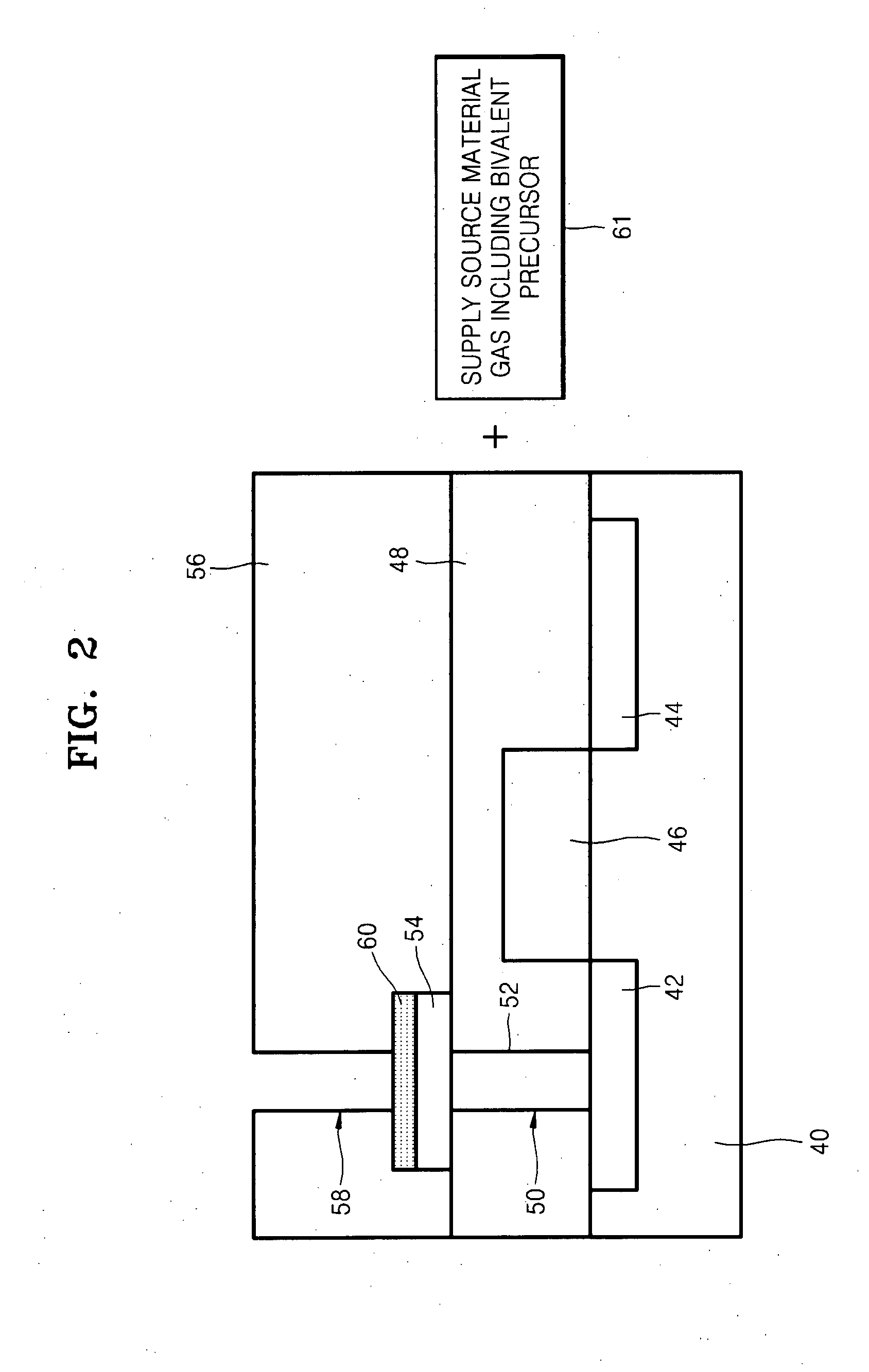
[0007] Example embodiments provide a method of forming a phase change layer and a method of manufacturing a storage node having the phase change layer. The method of forming a phase change layer may include providing a bivalent first precursor having germanium (Ge), providing a second precursor, and / or providing a third precursor onto a surface on which the phase change layer is to be formed using a deposition process. Additionally, the second precursor may have antimony (Sb), and the third precursor may have tellurium (Te). Furthermore, the phase change layer may be a Ge2Sb2Te5 (GST) layer.

[0008] The deposition process may be performed using chemical vapor deposition (CVD), which may include metal organic chemical vapor deposition (MOCVD) and cyclic chemical vapor deposition (cyclic-CVD). The deposition process may also be performed using atomic layer deposition (ALD). The composition (e.g., Ge, Sb, Te content) of the phase change layer may be controlled by regulating the depositi...


PUM

PropertyMeasurementUnit
Temperatureaaaaaaaaaa
Pressureaaaaaaaaaa
Areaaaaaaaaaaa

Abstract

A method of forming a phase change layer may include providing a bivalent first precursor having germanium (Ge), a second precursor having antimony (Sb), and a third precursor having tellurium (Te) onto a surface on which the phase change layer is to be formed. The phase change layer may be formed by CVD (e.g., MOCVD, cyclic-CVD) or ALD. The composition of the phase change layer may be varied by modifying the deposition pressure, deposition temperature, and/or supply rate of reaction gas. The deposition pressure may range from about 0.001-10 torr, the deposition temperature may range from about 150-350° C., and the supply rate of the reaction gas may range from about 0-1 slm. Additionally, the above phase change layer may be provided in a via hole and bounded by top and bottom electrodes to form a storage node.

Description

PRIORITY STATEMENT [0001] This application claims priority under 35 U.S.C. § 119(a) to Korean Patent Application No. 10-2006-0102463, filed on Oct. 20, 2006 in the Korean Intellectual Property Office (KIPO), the entire contents of which are incorporated herein by reference. BACKGROUND [0002] 1. Technical Field [0003] Example embodiments relate to a method of forming a phase change layer and a method of manufacturing a storage node having the phase change layer. [0004] 2. Description of the Related Art [0005] The resistance of a phase change material may vary depending to whether the phase change material is in a crystalline state or in an amorphous state. Additionally, the phase change material may change from a crystalline state to an amorphous state, and vice versa, depending on temperature. A phase change memory device may include a phase change layer made of the above-described phase change material as a means for storing bit data. An example of a phase change memory device may ...

Claims


Application Information

Patent Timeline
IPC IPC(8): H01L45/00C23C16/00
CPCC23C16/305H01L27/2436H01L45/06H01L45/1683H01L45/144H01L45/1616H01L45/1233H10B63/30H10N70/231H10N70/826H10N70/8828H10N70/023H10N70/066
Inventor SHIN, WOONG-CHULLEE, JAE-HOKANG, YOUN-SEON
Owner SAMSUNG ELECTRONICS CO LTD
Why Eureka
Try Eureka