Structure and method for dual surface orientations for CMOS transistors

Inactive Publication Date: 2008-05-15
GLOBALFOUNDRIES INC
View PDF12 Cites 9 Cited by
  • Summary
  • Abstract
  • Description
  • Claims
  • Application Information

AI Technical Summary

Benefits of technology

[0011]The present invention addresses the needs described above and provides methods of achieving

Problems solved by technology

Reduced transistor current results in deterioration of circuit stability and reduces the speed of circuit operation thereby causing degradation in performance.
A first general disadvantage of this type of approach is that the process of manufacture is prone to defect generation.
However, general difficulty in controlling the defect level in the selective epitaxy is known in the industry.
Even the use of recrystallization faces the challenge of generation of a boundary between two different surface orientations, where two different crystallographic orientations meet and generate substantial number of crystalline defects.
A second general disadvantage of this type of approach described above is that as a consequence of a high level of defect density near the boundaries, irrespective whether epitaxy is used or recrystallization is used, a substantial portion of the surface area becomes unusable for high performance CMOS devices.
This is because crystalline defects cause leakages in the CMOS

Method used


Image

  • Structure and method for dual surface orientations for CMOS transistors
  • Structure and method for dual surface orientations for CMOS transistors
  • Structure and method for dual surface orientations for CMOS transistors

Examples


first embodiment

[0094]According to the present invention, the substrate orientation is (100) , which is the optimal surface orientation for NFET devices while being the least desired orientation for PFET devices. The surface of the STI 370 may optionally be recessed by etching as shown in FIGS. 8A-8C to reduce topographic variations in the later stages of processing, particularly when the gate needs to be lithographically patterned. The etching process may utilize a wet etch or a reactive ion etch (RIE) to provide desired recess depth of the STI 370.

[0095]The NFET body 350 is masked with masking material 401 as schematically shown in FIGS. 9A-9C. The top surfaces of the unmasked PFET body 360 in FIGS. 7A-7C are subjected to etchant that produces surface orientations other than (100) . The resulting structure is described in FIGS. 9A-9C, which shows the etched PFET body 460 with facets 461 and ridges 462 where two facets with different surface orientations meet.

[0096]In FIG. 9A, the two rectangular ...

fourth embodiment

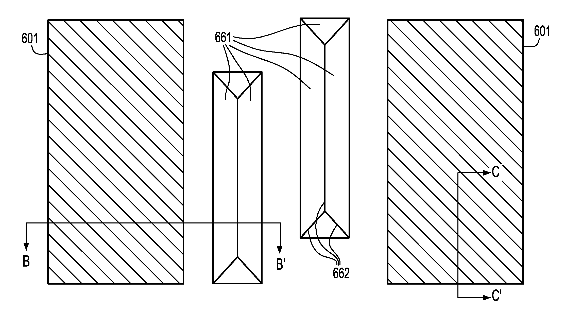
[0114]According to the present invention, the substrate is a (100) silicon substrate. The NFET body 350 as shown in FIGS. 7A-7C is masked with a masking material 601. The PFET body 360 is recessed by exposing them to etchant, either in a wet etch process or in a reactive ion etch process. The resulting structure with recessed PFET body 660 with a recessed silicon surface 659 are shown in FIGS. 13A-13C along with the masking material 601, an STI 370, the NFET body 350.

[0115]This is followed by a suitable surface pretreatment and then a selective epitaxy process that grows facets with surface orientations other than {100} orientations. The surface orientations of such facets are preferably {110}, {111}, {211}, {221} or {311}, and most preferably {110}. The resulting structure is described in FIGS. 14A-14C, which shows selective epitaxially grown PFET body 660 with facets 661 and ridges 662 where two facets with different surface orientations meet. After the formation of the selective ...

fifth embodiment

[0118]According to the present invention, the substrate is a (110) silicon substrate. The PFET body360 as shown in FIGS. 7A-7C is masked with a masking material. The NFET body in FIGS. 7A-7C is recessed by exposing them to etchant, either in a wet etch process or in a reactive ion etch process. This results in structures with recessed NFET body with a recessed silicon surface.

[0119]As in the fourth embodiment of the present invention, this is followed by a suitable surface pretreatment and then a selective epitaxy process that grows facets with surface orientations other than {110} orientations. The surface orientations of such facets are preferably {100}, {111}, {211}, {221} or {311}, and most preferably {100}. After the formation of the selective epitaxially grown NFET body, the masking material is removed. The process flow then follows the same processing steps as described in the first embodiment. The same requirement applies to the masking material in the fifth embodiment as in...


PUM


Abstract

The present invention provides structures and methods for providing facets with different crystallographic orientations than what a semiconductor substrate normally provides. By masking a portion of a semiconductor surface and exposing the rest to an anisotripic etch process that preferentially etches a set of crystallographic planes faster than others, new facets with different surface orientations than the substrate orientation are formed on the semiconductor substrate. Alternatively, selective epitaxy may be utilized to generate new facets. The facets thus formed are joined to form a lambda shaped profile in a cross-section. The electrical properties of the new facets, specifically, the enhanced carrier mobility, are utilized to enhance the performance of transistors. In a transistor with a channel on the facets that are joined to form a lambda shaped profile, the current flows in the direction of the ridge joining the facets avoiding any inflection in the direction of the current.

Description

FIELD OF THE INVENTION[0001]The present invention relates to semiconductor devices, and particularly, to complementary metal oxide semiconductor (CMOS) transistors.BACKGROUND OF THE INVENTION[0002]In each new generation of semiconductor technology, transistor current decreases due to gate width reduction, mobility degradation of minority carriers, and reduction of the supply voltage Vdd. Reduced transistor current results in deterioration of circuit stability and reduces the speed of circuit operation thereby causing degradation in performance. One of the key parameters determining the mobility of minority carriers is the crystallographic surface orientation on which the channel of the transistor is built. Therefore, the crystallographic orientation of the surface, or the surface orientation of a transistor structure plays a key role in determining the performance of the transistor.[0003]Specifically, the electron mobility in silicon is the highest for the {100} surface orientation ...

Claims


Application Information

Patent Timeline
IPC IPC(8): H01L29/04H01L21/311
CPCH01L21/02381H01L21/02433H01L21/02532H01L21/02609H01L29/7853H01L21/30608H01L21/823821H01L27/11H01L27/1104H01L21/02639H10B10/00H10B10/12
Inventor YANG, HAININGDYER, THOMAS W.WONG, KEITH KWONG HONYANG, CHIH-CHAO
Owner GLOBALFOUNDRIES INC
Why Eureka
Try Eureka