Scanning Device and Scanning Type Optical Apparatus
a scanning device and optical apparatus technology, applied in static indicating devices, non-linear optics, instruments, etc., can solve the problems of limiting the polygon mirror or galvano mirror, the configuration and control of the scanning system become complicated, and the scanning type image display apparatus does not have fixed pixels, etc., to suppress the load applied, the load applied is less deflected, and the load applied is suppressed.
- Summary
- Abstract
- Description
- Claims
- Application Information
AI Technical Summary
Benefits of technology
Problems solved by technology
Method used
Image
Examples
first embodiment
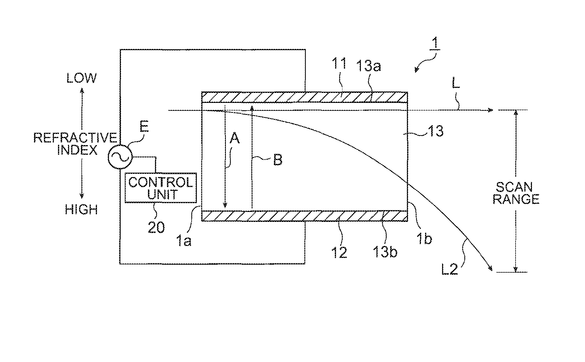
[0045]In a scanning device 1, the refractive-index distribution changes according to the intensity of an electric field generated therein, such that a laser beam propagating therethrough is scanned. Specifically, as shown in FIG. 1, the scanning device 1 includes a first electrode 11, a second electrode 12; an optical element 13, and a control unit 20.
[0046]The optical element 13 is dielectric crystal (electro optic crystal) having an electro optic effect. In the present embodiment, the optical element 13 is formed of a crystal material having the composition of KTN (potassium tantalate niobate; KTa1-xNbxO3) Moreover, the KTN crystal is crystal using the Kerr effect (a phenomenon in which birefringence occurs when an electric field is applied to an isotropic material and the effect is proportional to the square of the intensity of an electric field generated by an applied voltage).
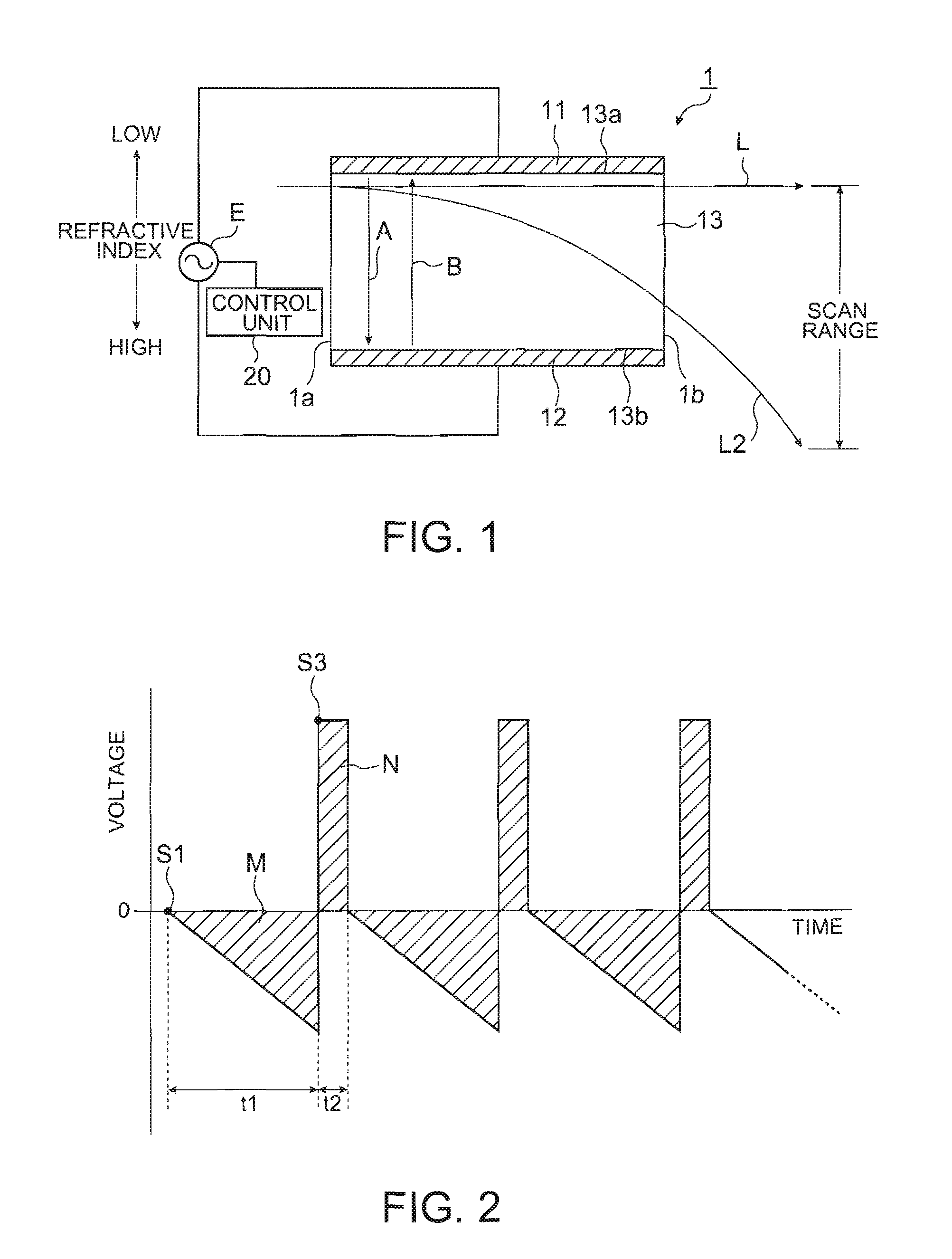
[0047]In addition, the optical element 13 has a rectangular parallelepiped shape. The first electrode 1...
second embodiment
[0063]Next, a second embodiment of the invention will be described with reference to FIGS. 3 and 4. In addition, in each embodiment to be described below, components common to those in the scanning device according to the first embodiment are denoted by the same reference numerals, and the description thereof will be omitted.
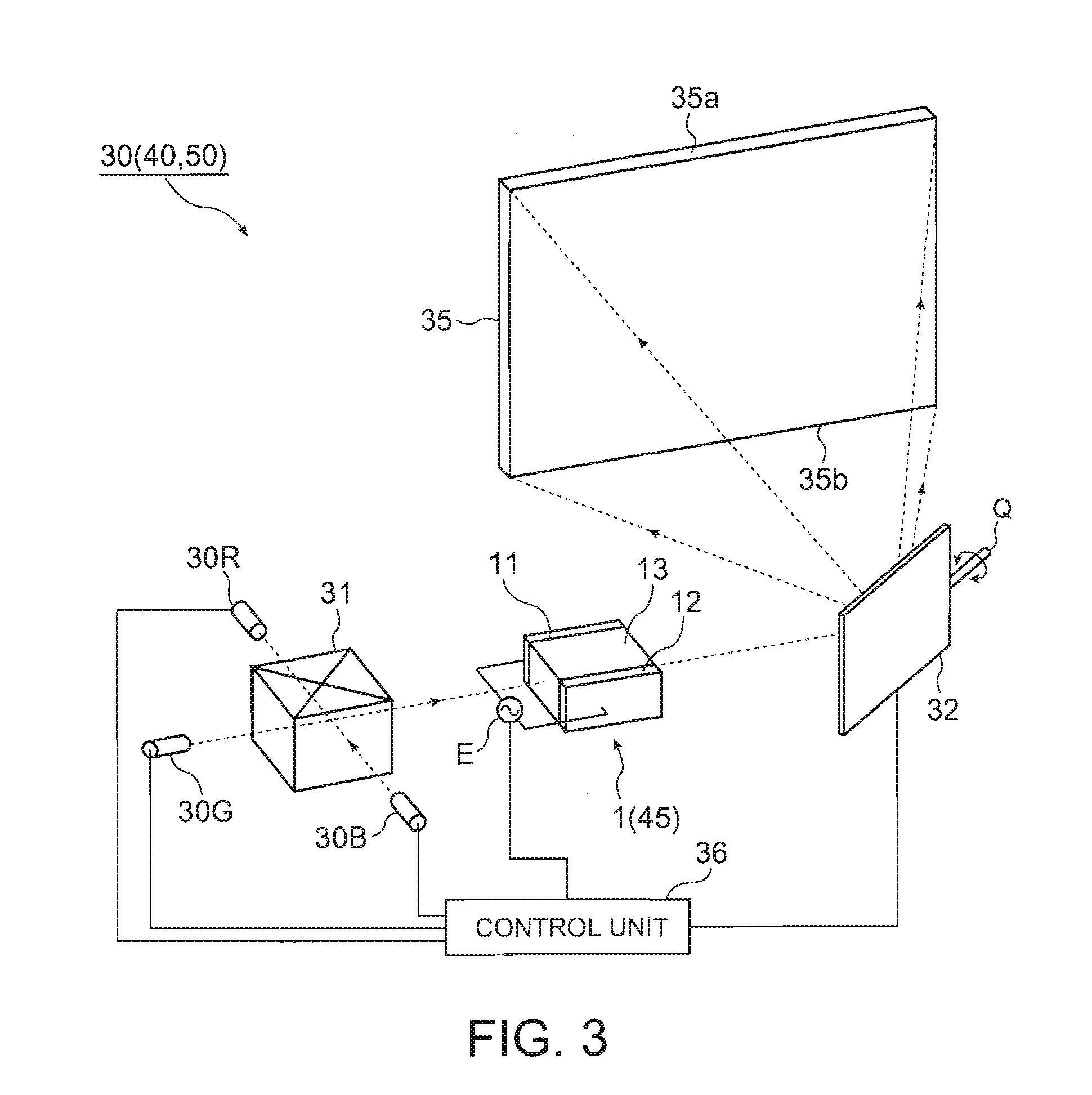
[0064]In the present embodiment, an image display apparatus (scanning type optical apparatus) 30 including the scanning device 1 according to the first embodiment as a scanning unit will be described.
[0065]As shown in FIG. 3, an image display apparatus 30 includes: a red-colored light source (light source) 30R that emits a red-colored laser beam; a green-colored light source (light source) 30G that emits a green-colored laser beam; a blue-colored light source (light source) 30B that emits a blue-colored laser beam; a cross dichroic prism 31; the scanning device 1 that scans a laser beam emitted from the cross dichroic prism 31 in a horizontal direction of a scre...
third embodiment
[0076]Next, a third embodiment of the invention will be described with reference to FIGS. 3 to 5.
[0077]The entire configuration of an image display apparatus 40 according to the present embodiment is the same as that of the image display apparatus shown in FIG. 3 except for a voltage applied to the second electrode 12 of the scanning device 1. Accordingly, this different point will now be described.
[0078]Hereinafter, scanning of laser beams emitted from the red, green, and blue colored light sources 30R, 30G, and 30B will be described.
[0079]As shown in FIG. 3, a laser beam emitted from a scanning device 45 is scanned from an upper end 35a to a lower end 35b of the screen 35 by means of the galvano mirror 32 and then returns to the upper end 35a of the screen 35 again. Thus, a period for which a laser beam returns from the lower end 35b to the upper end 35a of the screen 35, that is, a period for which the galvano mirror 32 returns from a position, at which the rotation angle of the ...
PUM
| Property | Measurement | Unit |
|---|---|---|
| voltages | aaaaa | aaaaa |
| voltages | aaaaa | aaaaa |
| voltage | aaaaa | aaaaa |
Abstract
Description
Claims
Application Information


