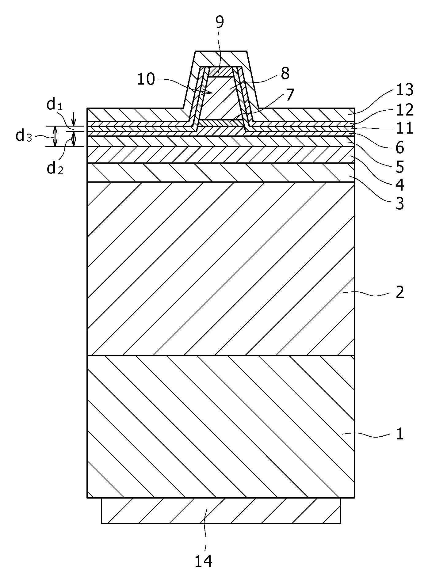
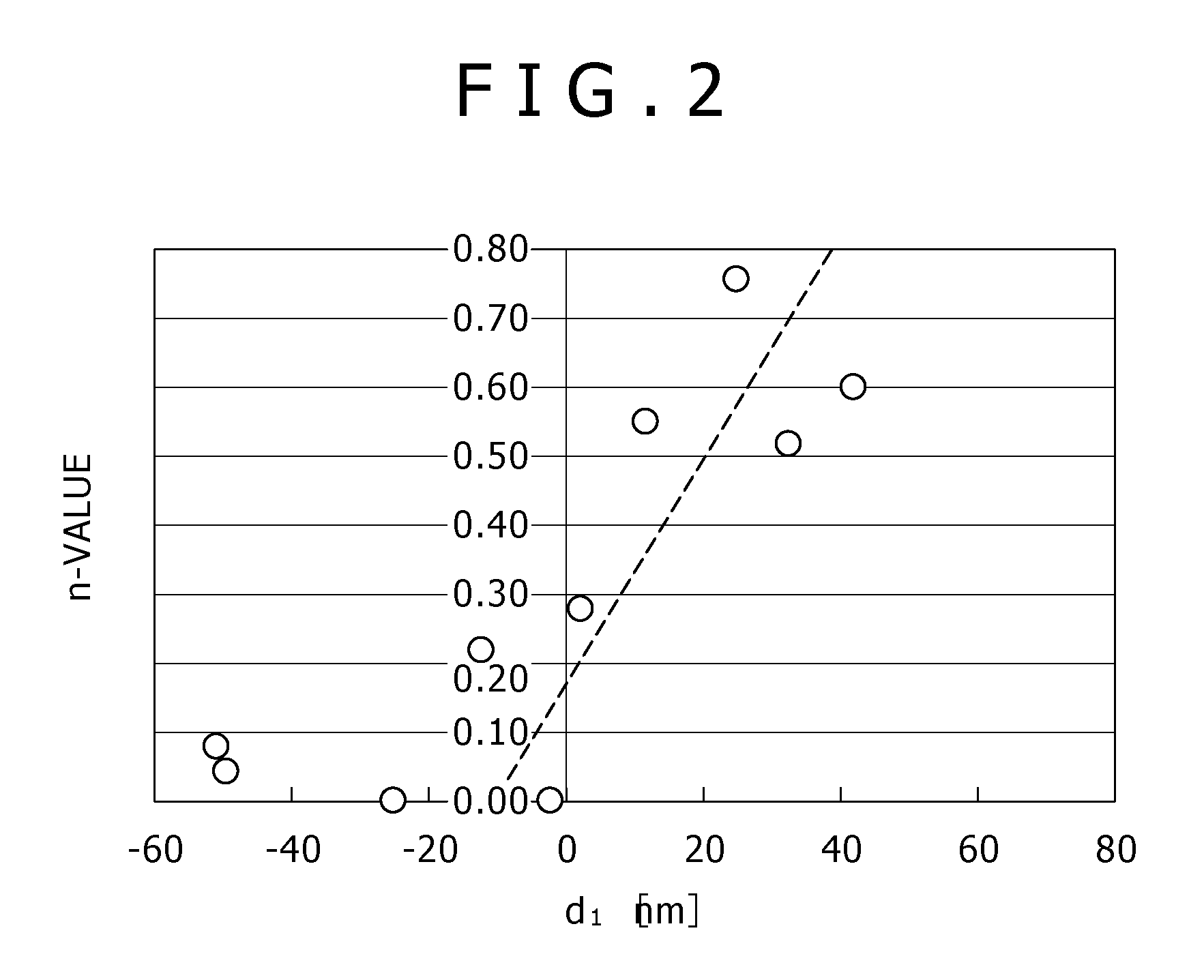
[0042]From the viewpoint of more assured prevention of the semiconductor laser from deterioration, the distance between the electron barrier layer and a bottom surface in areas on both side of the ridge stripe is preferably not less than 20 nm. On the other hand, from the viewpoint of prevention of the
active layer from being deteriorated due to damages introduced to the bottom surface in the areas on both side of the ridge stripe upon formation of the ridge stripe, the distance from the bottom surface in the areas on both sides of the ridge stripe and the active layer is preferably not less than 100 nm. In addition, from the
viewpoints of reducing internal loss of the semiconductor laser, reducing the
threshold current and enhancing the
slope efficiency, the distance between the electron barrier layer and the active layer is preferably not less than 110 nm. On the other hand, if the distance between the electron barrier layer and the active layer exceeds 300 nm, the internal
quantum efficiency is lowered. Therefore, the distance between the electron barrier layer and the active layer is preferably not more than 300 nm.
[0046]Taking this point into consideration, the present inventor made intensive and extensive investigations. As a result of the investigations, it was found out that the p-side
electrode 113 in the vicinity of a
resonator end face after the cleavage can be prevented from being partly or completely exfoliated from the p-type GaN
contact layer 109, by using a metallic laminate film including n
metal films (n is an integer of not less than 2) as an
electrode formed without any alloying step on a ridge stripe, more generally a nitride type Group III-V compound semiconductor layer, setting the
total thickness of the metallic laminate film to be not less than 300 nm, and setting the equivalent mean modulus of rigidity defined for the metallic laminate film in the following manner to be not more than 55 GPa. More specifically, in the case of forming a p-side
electrode on a ridge stripe without carrying out any alloying treatment at the interface between them, a configuration in which at least a part of the p-side electrode includes a metallic laminate film including n
metal films (n is an integer of not less than 2), wherein the
total thickness of the metallic laminate film is not less than 300 nm, and the equivalent mean modulus of rigidity, Ge, of the metallic laminate film defined by the following formula:Ge=∑i=1nGi×ti∑i=1nti[Math1]where Gi and ti represent the modulus of rigidity and the thickness of the i-th
metal film as numbered from the bottom side of the metallic laminate film, satisfies the condition of Ge≦55 GPa, is effective in preventing the exfoliation of the p-side electrode. Preferably, but not limitatively, the
total thickness of the metallic laminate film constituting the p-side electrode is not less than 500 nm, and Ge≦50 GPa.
[0052]In the case of forming the grooves on both sides of the ridge stripe and forming the p-side electrode in the state of extending even to the outer sides of the grooves, the thickness of the part over the
contact layer in the areas on the outer sides of the grooves, of the insulating film which is formed on the side surfaces of the ridge stripe and in the inside of the grooves and over the
contact layer in the areas on the outer sides of the grooves, is made to be sufficiently large. This configuration ensures that the distance between the p-side electrode and the n-side electrode in the areas on the outer sides of the grooves can be set larger as compared with the distance in the areas of the ridge stripe or the grooves, so that it is possible to contrive a reduction in the electrostatic capacity between the electrodes, to contrive enhancement of high-frequency characteristics of the semiconductor laser, and to prevent electrostatic leak and electrostatic breakdown.
[0054]In the first to fourth embodiments of the present invention configured as above-mentioned, the ridge stripes are each formed at an upper part of the p-side optical waveguide layer, the electron barrier layer and the p-side clad layer, and the distance between the electron barrier layer and the bottom surface in areas on both sides of the ridge stripe is not less than 10 nm. In other words, the electron barrier layer is entirely included in the ridge stripe, and the distance between the electron barrier layer and the bottom surface in the areas on both sides of the ridge stripe is not less than 10 nm. This configuration makes it possible to prevent damages generated in forming the ridge stripes by
dry etching from being generated in the electron barrier layer or the p-side optical waveguide layer therebeneath.
[0055]According to an embodiment of the present invention, the damages generated in forming the ridge stripes by
dry etching can be prevented from being generated in the electron barrier layer or the p-side optical waveguide layer therebeneath. Therefore, a semiconductor laser using a nitride type Group III-V compound semiconductor and having a high reliability and a long life, irrespectively of dispersions of
etching in a
dry etching step, can be realized while maintaining a low
threshold current and a high
slope efficiency characteristic, by appropriately setting the distance between the active layer and the electron barrier layer. With this semiconductor laser used as a
light source, furthermore, a high-performance optical disk
system can be realized.

