Method of forming a structure having a high dielectric constant, a structure having a high dielectric constant, a capacitor including the structure, a method of forming the capacitor

a technology of dielectric constant and structure, applied in the direction of fixed capacitors, fixed capacitor details, synthetic resin layered products, etc., can solve the problems of high leakage, high leakage, and the inability of cvd to provide good step coverage and film stoichiometry in high fill aspect ratio containers

Inactive Publication Date: 2008-05-22
MICRON TECH INC
View PDF16 Cites 22 Cited by
  • Summary
  • Abstract
  • Description
  • Claims
  • Application Information

AI Technical Summary

Problems solved by technology

With the continual shrinkage of microelectronic devices, such as capacitors, the materials traditionally used in integrated circuit technology are approaching their performance limits.
However, when a thin film of SiO2 is formed, such as less than 5 nm in thickness, the film has defects, which leads to high ...

Method used


Image

  • Method of forming a structure having a high dielectric constant, a structure having a high dielectric constant, a capacitor including the structure, a method of forming the capacitor
  • Method of forming a structure having a high dielectric constant, a structure having a high dielectric constant, a capacitor including the structure, a method of forming the capacitor
  • Method of forming a structure having a high dielectric constant, a structure having a high dielectric constant, a capacitor including the structure, a method of forming the capacitor

Examples


example

Example 1

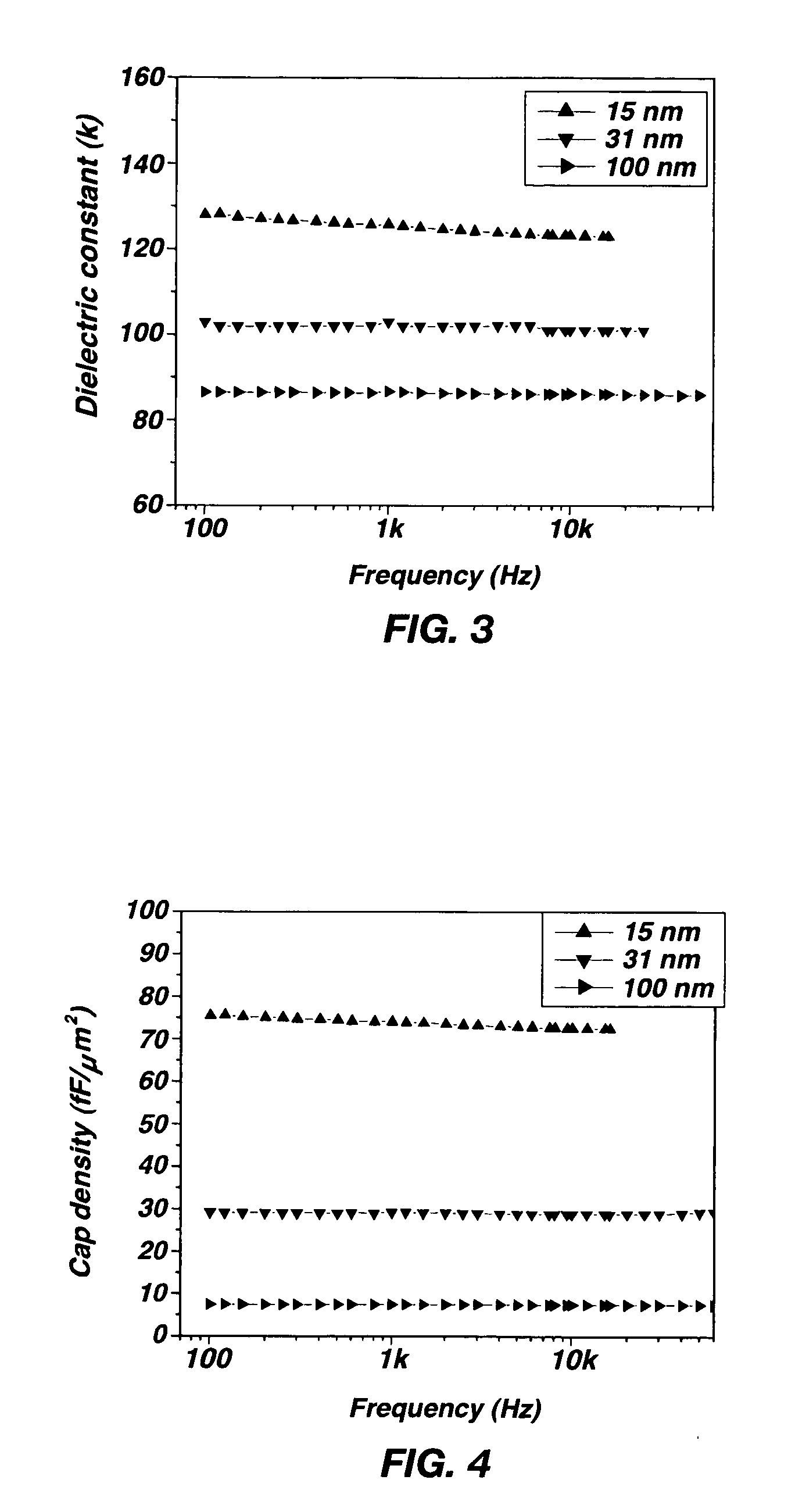
[0027]Formation and Electrical Properties of 15 nm, 31 nm, and 100 nm STO Films

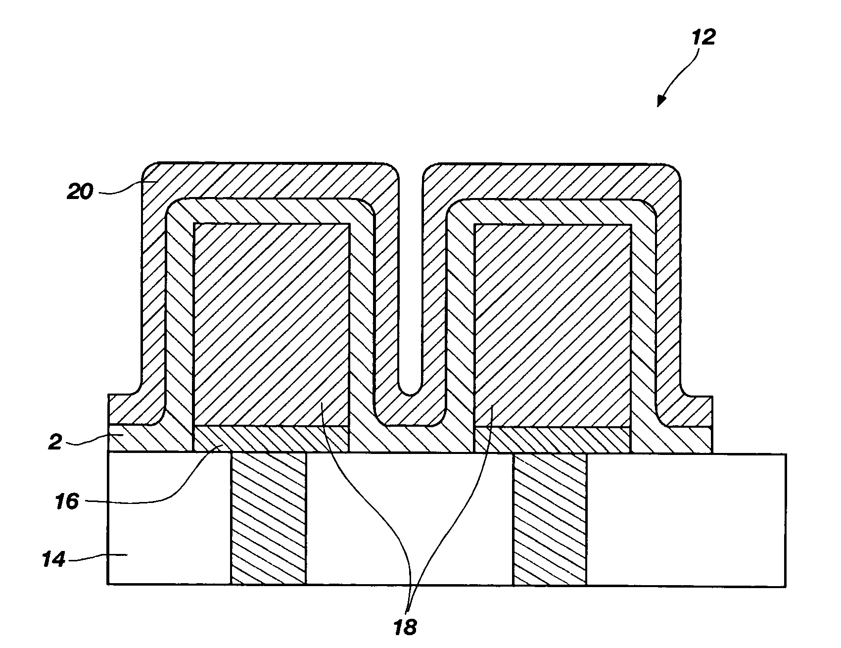
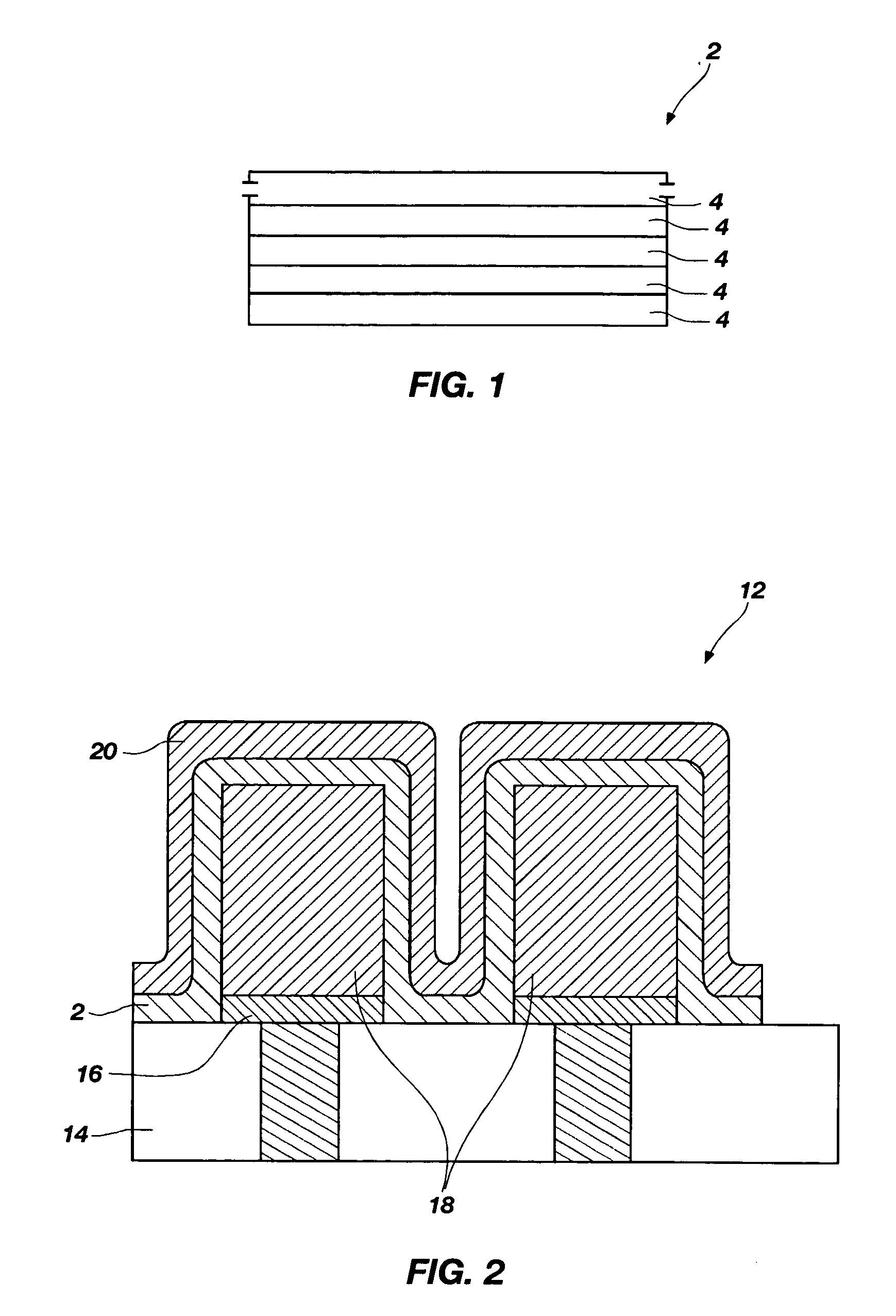
[0028]STO stacks having an STO film positioned between two layers of platinum were formed. Each layer of platinum (“Pt”) was sputter-deposited to a thickness of 30 nm. STO films having a total thickness of 15 nm, 31 nm, or 100 nm were formed by conducting multiple ALD and anneal cycles, with each ALD and anneal cycle producing a portion of the STO film.

[0029]To form the 15 nm STO film, a 5 nm portion of the STO material was deposited by ALD at 300° C. on a first platinum layer. Each portion of the STO material was deposited as follows:[0030]Ti precursor pulse (60 sec) / purge (30 sec) / oxidizer O3 (30 sec) / purge (20 sec)=1 TiO2 cycle[0031]Sr precursor pulse (30 sec) / purge (30 sec) / oxidizer 03 (30 sec) / purge (30 sec)=1 SrO cycle[0032]Sr Flow: 0.8 ml / min, 30 sec-60 sec[0033]Ti Flow: 0.8 ml / min, 40 sec-60 sec[0034]THF: 0.4 ml / min-1.0 ml / min, 15 sec-30 sec[0035]O3 concentration: 15% by volume[0036]O3 f...


PUM

PropertyMeasurementUnit
Temperatureaaaaaaaaaa

Abstract

A method of forming a dielectric structure, such as a layer, is disclosed. The method comprises forming a high-k structure from a plurality of portions of a high-k material. Each of the plurality of portions of the high-k material is formed by depositing a plurality of monolayers of the high-k material and annealing the high-k material. The high-k material may be a perovskite-type material including, but not limited to, strontium titanate. A dielectric structure, a capacitor incorporating a dielectric structure and a method of forming a capacitor are also disclosed.

Description

FIELD OF THE INVENTION[0001]Embodiments of the invention relate to forming a structure having a high dielectric constant (k) and a low leakage current. Specifically, embodiments of the invention relate to forming the structure having the high k and low leakage current from a perovskite-type material.BACKGROUND OF THE INVENTION[0002]Capacitors are the basic energy storage devices in random access memory devices, such as dynamic random access memory (“DRAM”) devices. Capacitors include two conductors, such as parallel metal or polysilicon plates, which act as electrodes. The electrodes are insulated from each other by a dielectric material. With the continual shrinkage of microelectronic devices, such as capacitors, the materials traditionally used in integrated circuit technology are approaching their performance limits. Silicon dioxide (“SiO2”) has frequently been used as the dielectric material in capacitors. However, when a thin film of SiO2 is formed, such as less than 5 nm in th...

Claims


Application Information

Patent Timeline
IPC IPC(8): B05D5/12H01G9/00H01G4/005
CPCH01G4/12Y10T29/417H01L27/10852H01G4/1218H10B12/033H01L21/02H10B99/00
Inventor SRINIVASAN, BHASKARSMYTHE, JOHN A.
Owner MICRON TECH INC
Why Eureka
Try Eureka