Nitride semiconductor material, semiconductor element, and Manufacturing method thereof

a technology of nitride semiconductor and semiconductor element, which is applied in the direction of semiconductor devices, semiconductor/solid-state device details, electrical apparatus, etc., can solve the problems of difficulty in designing an optimal band structure for the performance characteristic of the element, difficulty in controlling the irregularities of the interface caused by impurities, and difficulty in improving the high frequency characteristics of the device. , to achieve the effect of promoting atomic migration in the interface and controlling irregularities in the interfa

Active Publication Date: 2008-05-29
PANASONIC CORP
View PDF5 Cites 25 Cited by
  • Summary
  • Abstract
  • Description
  • Claims
  • Application Information

AI Technical Summary

Benefits of technology

[0048]Accordingly, by depositing the group IV nitride without extraction from the furnace, mixing-in of impurities such as oxygen in the interface between the group IV nitride and the group III nitride semiconductor can be suppressed to a minimum, and irregularities in the interface caused by impurities can be controlled. Moreover, by depositing the group IV nitride by thermal decomposition reaction, atomic migration in the interface can be promoted. Accordingly, the two-dimensional growth of the group IV nitride can be promoted while suppressing the three-dimensional growth of the group IV nitride.
[0049]The present invention can provide a nitride semiconductor material and a semiconductor element which enable the designing of an optimal band structure for the behavior characteristics of the element, and a manufacturing method thereof.

Problems solved by technology

However, although excellent high frequency characteristics can be realized with the conventional semiconductor element such as a GaN-based MIS-type transistor, the mechanism for increasing carrier density is unclear.
Accordingly, improvement of high frequency characteristics of a device, such as further increasing the carrier density and reducing sheet resistance, is difficult.
In other words, with a conventional semiconductor element, it is difficult to design an optimal band structure for the performance characteristic of the element.

Method used


Image

  • Nitride semiconductor material, semiconductor element, and Manufacturing method thereof
  • Nitride semiconductor material, semiconductor element, and Manufacturing method thereof
  • Nitride semiconductor material, semiconductor element, and Manufacturing method thereof

Examples


first embodiment

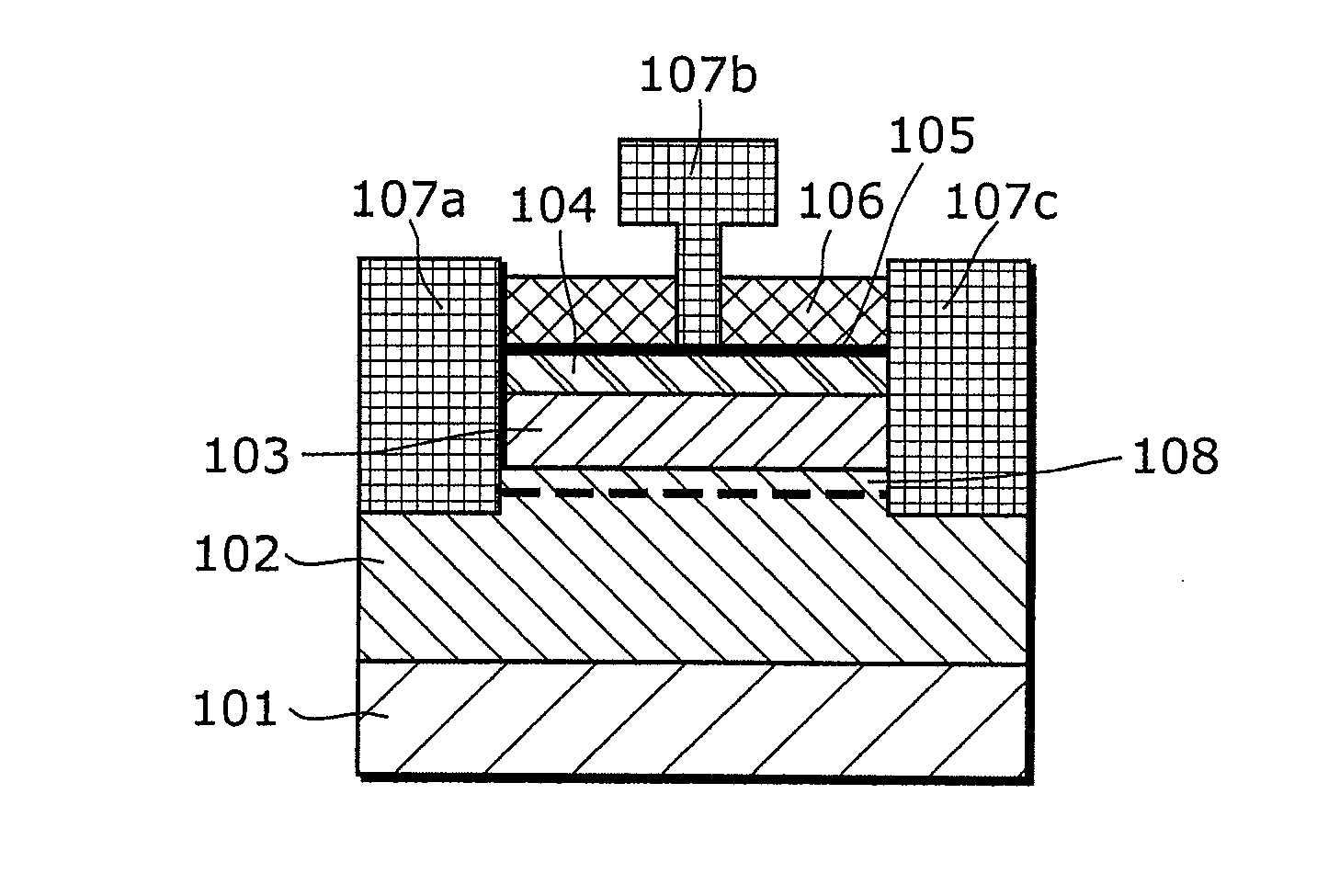
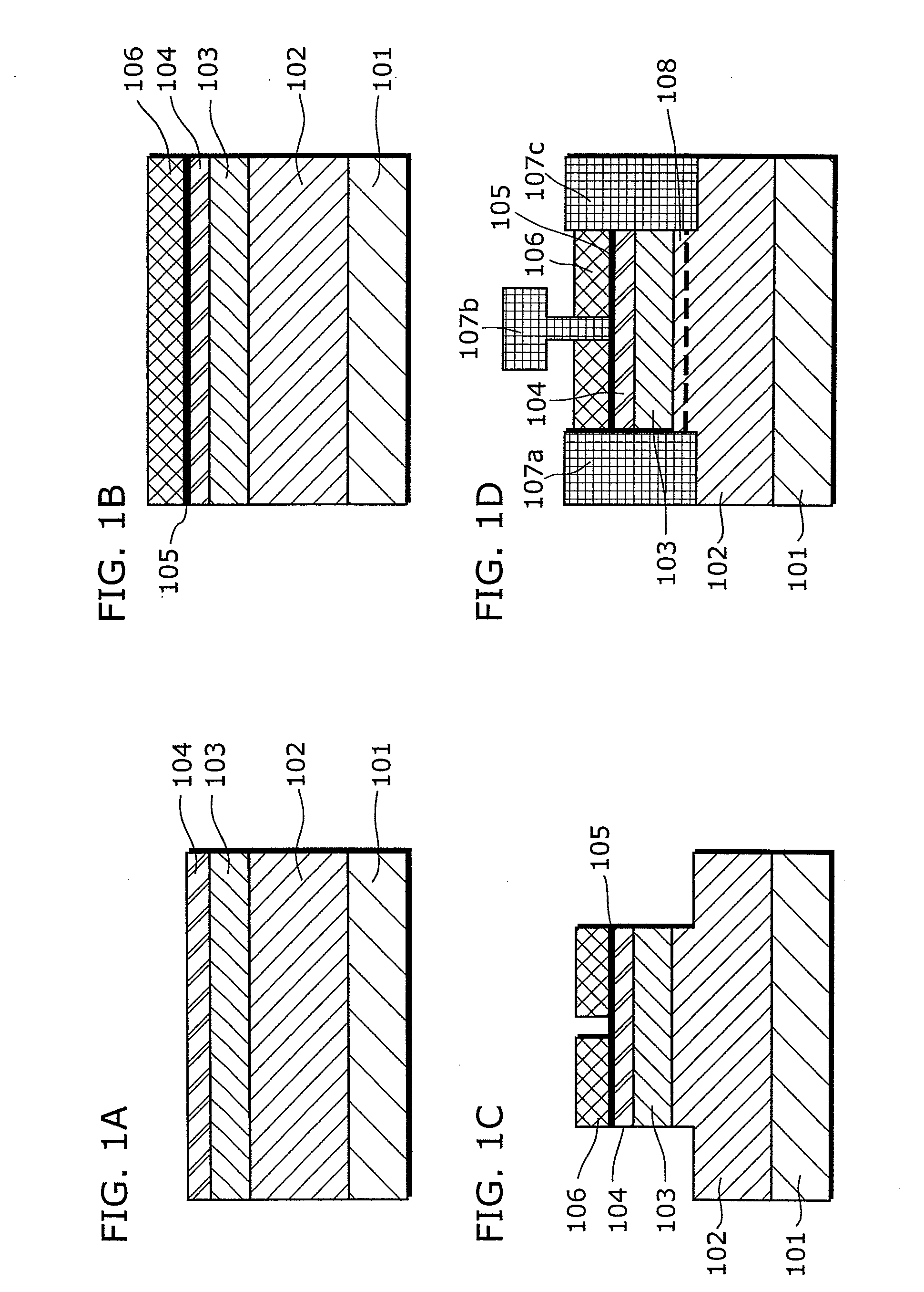
[0079]In the first embodiment of the present invention, a manufacturing method of a semiconductor element that uses a nitride semiconductor material in which an interface between a group III nitride semiconductor and a group IV nitride becomes a regular atomic arrangement will be explained.

[0080]The semiconductor element that uses the nitride semiconductor material according to the first embodiment of the present invention is formed by using crystal growth technology. In the semiconductor element that uses the nitride semiconductor material according to the first embodiment, group III raw material of the group III nitride semiconductor uses trimethyl gallium (hereafter, called TMG) for example as a gallium raw material, trimethyl aluminum (hereafter, called TMA) for example as an aluminum raw material, and trimethyl indium (hereafter, called TMI) for example as an indium raw material. Moreover, as a group V raw material, ammonia (hereafter, called NH3) for example is used as a nitro...

second embodiment

[0097]In the second embodiment of the present invention, explanation is carried out regarding an interface structure for the precise controlling of dangling bonds for the purpose of improving the degree of freedom in materials design in the combination of a group III nitride semiconductor and various group IV nitrides, and efficiently imparting strain-induced stress.

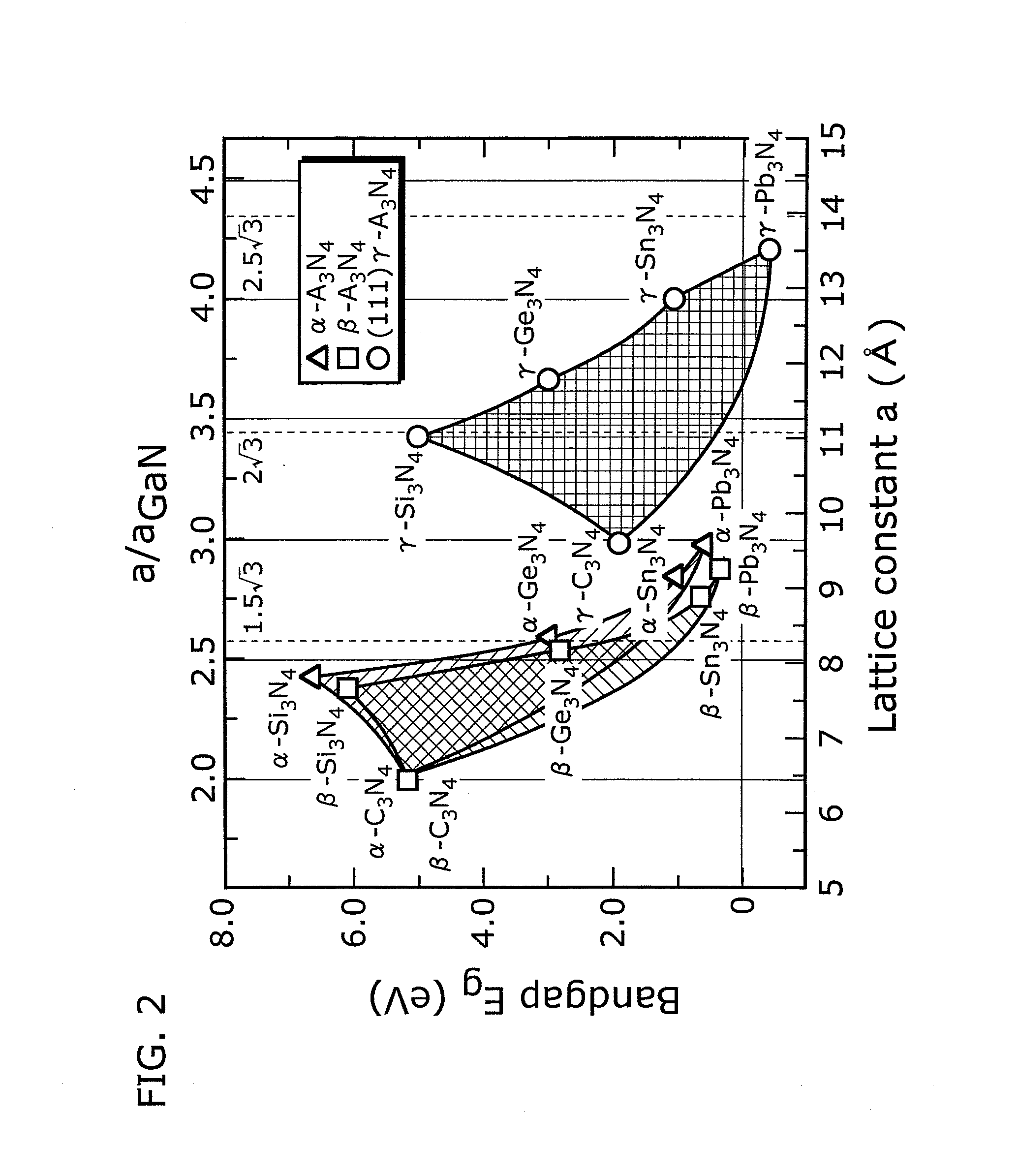
[0098]The lattice constant and the band gap of the group IV nitride can be freely designed by including one or more of carbon, silicon, germanium, tin, and lead, as the group IV element. We obtained, through first principle calculation, the relation between the lattice constant and the band gap when various group IV elements are used in the group IV nitride. The result is shown in FIG. 2. FIG. 2 is a diagram showing the relation between the lattice constant and the band gap in three crystal structures (alpha-phase structure, beta-phase structure, and gamma-phase structure) taken by the group IV nitride. By modulating the...

third embodiment

[0120]In the third embodiment of the present invention, explanation will be carried out regarding a semiconductor element that enables, through a group IV nitride, in-plane anisotropy in the interface of the group III nitride semiconductor. Two examples of enabling in-plane anisotropy in the interface of the group III nitride semiconductor, through a group IV nitride will be explained as follows.

[0121]First, an example in which trench configurations are formed in the group III nitride semiconductor so as to enable anisotropy in the interface with the group IV nitride will be explained. FIG. 7A is a perspective view showing the structure of a field-effect transistor device in which trench configurations are formed in the group III nitride semiconductor so as to enable anisotropy in the interface with the group IV nitride. The field-effect transistor device shown in FIG. 7A includes a (0001) plane GaN substrate 701, an undoped GaN layer 702, a silicon nitride film 703, a source electr...


PUM

PropertyMeasurementUnit
Cut-off aaaaaaaaaa
sheet carrier densityaaaaaaaaaa
thicknessaaaaaaaaaa

Abstract

The nitride semiconductor material according to the present invention includes a group III nitride semiconductor and a group IV nitride formed on the group III nitride semiconductor, where an interface between the group III nitride semiconductor and the group IV nitride has a regular atomic arrangement. Moreover, an arrangement of nitrogen atoms of the group IV nitride in the interface and an arrangement of group III atoms of the group III nitride semiconductor in the interface may be substantially identical.

Description

BACKGROUND OF THE INVENTION[0001](1) Field of the Invention[0002]The present invention relates to a nitride semiconductor material, a semiconductor element, and a manufacturing method thereof. In particular, the present invention relates to a nitride semiconductor material and a semiconductor element which are made of a group III nitride semiconductor and a group IV nitride, and a manufacturing method thereof.[0003](2) Description of the Related Art[0004]Recently, research and development of an electronic device such as a transistor made of a group III nitride semiconductor, for example, GaN is being widely carried out. Since a band gap of GaN is large, and a saturated drift velocity of the electron of GaN is high, GaN offers much promise for high power high frequency electron devices. For example, a semiconductor element that uses GaN is described in Japanese Laid-Open Patent Application No. 2004-228481. Moreover, it is reported that it is possible to obtain a large value of 152 GH...

Claims


Application Information

Patent Timeline
Patent Type & Authority Applications(United States)
IPC IPC(8): H01L29/20H01L21/205
CPCH01L21/0254H01L21/02609H01L21/02664H01L21/3185H01L29/7787H01L29/2003H01L29/24H01L29/267H01L29/045H01L21/02271H01L21/0217
Inventor TAKIZAWA, TOSHIYUKIUEDA, TETSUZO
Owner PANASONIC CORP
Why Eureka
Try Eureka